Manufacturing method for printed circuit board

A technology for printed circuit boards and manufacturing methods, which is applied in the direction of multilayer circuit manufacturing and electrical connection formation of printed components, which can solve problems such as low reliability, shortened production cycle, and difficult alignment, so as to reduce wiring density and reduce safety. Distance, the effect of increasing the wiring density

Active Publication Date: 2014-04-09
SHANGHAI MEADVILLE SCI & TECH +1
View PDF4 Cites 12 Cited by
  • Summary
  • Abstract
  • Description
  • Claims
  • Application Information

AI Technical Summary

Problems solved by technology

[0009] The purpose of the present invention is to provide an effective and reliable method for producing multi-level high-density printed circuit boards, which can use existing materials and equipment and adopt a one-time pressing method, which can effectively shorten the production cycle and save

Method used


Image

  • Manufacturing method for printed circuit board
  • Manufacturing method for printed circuit board
  • Manufacturing method for printed circuit board

Examples


Embodiment 1

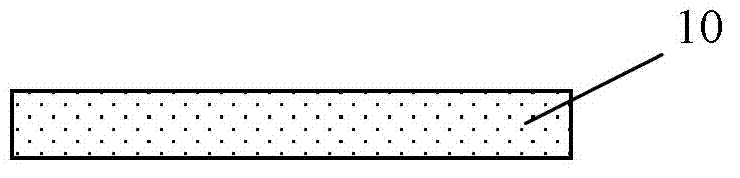
[0055] Step 1, such as Figure 8 As shown, an insulating dielectric material 1 with a protective film is laminated on a metal foil (copper foil) 2 .

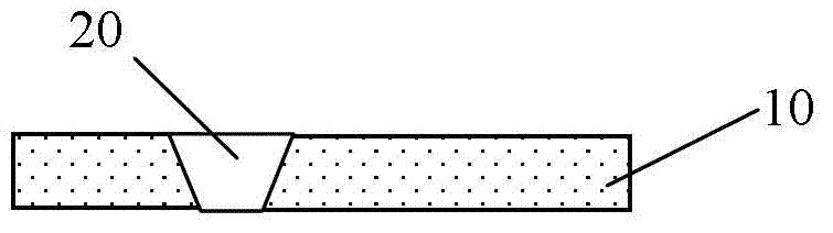
[0056] Step 2, such as Figure 9 As shown, a via hole 3 is formed on the above-mentioned insulating dielectric material 1 with a protective film. The hole is generally processed by laser, which can be carbon dioxide laser or UV laser.

[0057] Step 3, such as Figure 10 As shown, the conductive material 4 is filled in the above-mentioned via hole, and then the protective film is removed; the conductive material is generally a paste or slurry containing metal particles, and the metal particles include but are not limited to copper, silver, iron, etc.; the hole filling method can be The conventional ordinary screen printing method can also be used for vacuum screen printing.

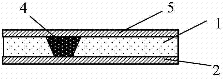
[0058] In the 4th step, a metal foil 5 is placed on the surface of the insulating dielectric material 1 filled with the conductive material 4, such as ...

Embodiment 2

[0066] Step 1, such as Figure 19 As shown, an insulating dielectric material 1 with a protective film is laminated on a metal foil (copper foil) 2 .

[0067] Step 2, such as Figure 20 As shown, a via hole 3 is formed on the above-mentioned insulating dielectric material 1 with a protective film. The hole is generally processed by laser, which can be carbon dioxide laser or UV laser.

[0068] Step 3, such as Figure 21 As shown, the conductive material 4 is filled in the above-mentioned via hole 3, and then the protective film is removed; the conductive material is generally a paste or paste containing metal particles, and the metal particles include but are not limited to copper, silver, iron, etc.; the hole filling method You can use the conventional common screen printing method, or you can use vacuum screen printing.

[0069] In the 4th step, a metal foil 5 is placed on the surface of the insulating dielectric material 1 filled with the conductive material 4, such as ...


PUM


Abstract

The invention relates to a manufacturing method for a printed circuit board, wherein manufacturing of a multi-layer high-density interconnected printed circuit board can be realized by using the one-time compressing method. The method comprises the following steps that: first daughter boards and second daughter boards are manufactured; the plurality of first daughter boards and daughter boards are superposed together and heating and pressurizing are carried out, and thus the first daughter boards and the second daughter boards are bonded together to form a multi-layer and multi-stage printed circuit board; conventional processes like mechanical drilling, hole metallization, and electroplating and the like are carried out on the multi-layer printed circuit board so as to complete the manufacturing of the printed circuit board. According to the invention, expansion and shrinkage as well as deformation of materials during the manufacturing process can be effectively controlled, thereby effectively improving alignment precision between the holes and between the hole and the graph; and the safe distances between the holes and between the hole and the graph are reduced from 20 mil to 8mil, thereby effectively improving the wiring density of the printed circuit board. Moreover, under the circumstances that the investment of the PCB manufacturer equipment is not increased, the yield of the high-density interconnected printed circuit board can be substantially improved and the manufacturing period of the product can be shortened.

Description

technical field [0001] The invention relates to a method for manufacturing a printed circuit board, in particular to a method for manufacturing a printed circuit board based on a one-time lamination process and realizing interlayer interconnection through plugging holes of conductive substances. Background technique [0002] Moore's Law states that the number of transistors that can be accommodated on an IC will double every 18 months, and the performance will also double; following this law, electronic products are currently moving towards high speed, multi-function, and miniaturization And the development of light weight, the development of corresponding IC packaging must also follow the development of electronic products and IC design towards the development of multi-pin count, miniaturization, thinning and high heat dissipation, as the motherboard used for mounting package substrates Printed printed circuit boards (PCBs) must also develop in the direction of lightness, t...

Claims


Application Information

Patent Timeline
IPC IPC(8): H05K3/40H05K3/46
Inventor 罗永红任潇璐吴金华陈培峰付海涛罗辉黄伟
Owner SHANGHAI MEADVILLE SCI & TECH
Why Eureka
Try Eureka