Manufacturing method of micro-fluid channel

A microfluidic channel and microchannel technology, applied in the field of microfabrication, can solve the problems of easily polluting the environment, cumbersome, high cost, and achieve the effects of fast and simple preparation process, improved etching efficiency, and reduced usage

Inactive Publication Date: 2014-04-16
XIAOSHAN BIOENG CENT OF YANGTZE DELTA REGION INST OF TSINGHUA UNIV ZHEJIANG
View PDF5 Cites 11 Cited by
  • Summary
  • Abstract
  • Description
  • Claims
  • Application Information

AI Technical Summary

Problems solved by technology

[0004] However, in the process of processing microchannels by wet etching, a sacrificial layer with microchannel patterns must first be processed on the surface of the substrate by photolithography. The material of the sacrificial layer is generally metals such as chromium, gold, platinum and photoresist. Layer patterns are generally processed by photolithography, and the steps involved in mask making, exposure and development require expensive instruments, ultra-clean room environments, and cumbersome preparation processes, so they cannot meet the needs of rapid and mass production; secondly, the traditional Wet etching is often achieved by immersing the substrate in a large amount of etching solution system combined with mechanical stirring. Therefore, before wet etching, some methods must be used to protect the back of the substrate and other areas that do not need to be processed. , very cumbersome; in addition, these etching solutions used in the preparation of microchannels are mostly strong acids, strong alkalis or toxic organic solvents, which are easy to pollute the environment, waste liquid treatment is very cumbersome, and the cost is high

Method used


Image

  • Manufacturing method of micro-fluid channel
  • Manufacturing method of micro-fluid channel
  • Manufacturing method of micro-fluid channel

Examples


Embodiment 1

[0023] Embodiment 1 Preparation of a linear glass microchannel

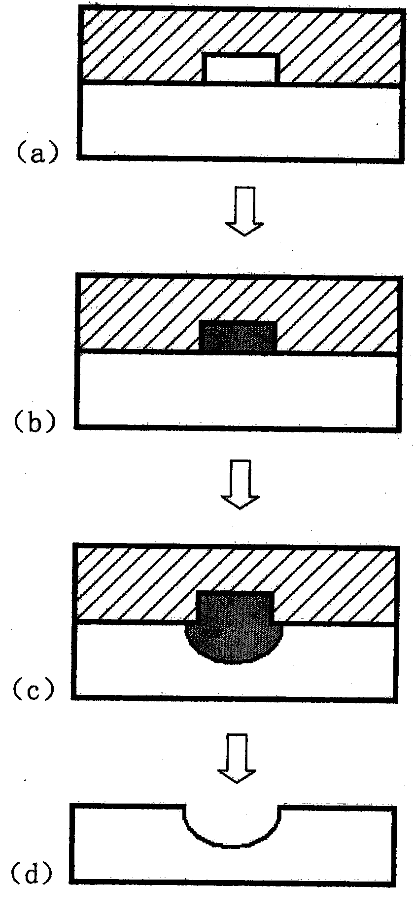
[0024] figure 1 It is a schematic diagram of the processing process of a microchannel provided by the present invention. The specific preparation process is as follows: firstly, a microchannel structure is processed on a smooth and flat polytetrafluoroethylene substrate using precision numerical control CNC engraving technology, and then the substrate and the surface of the flat glass to be processed are reversibly bonded ( figure 1 a); Then use the external peristaltic pump system to continuously introduce the hydrofluoric acid etching solution into the microchannel along a polytetrafluoroethylene hose ( figure 1 b); Hydrofluoric acid etchant etches the area where the microchannel is located on the glass substrate to the desired depth ( figure 1 c); Finally, the polytetrafluoroethylene substrate is peeled off from the surface of the glass substrate to obtain a glass microchannel.

[0025] More specifically, t...

Embodiment 2

[0026] Embodiment 2 Preparation of a cross-shaped glass microchannel

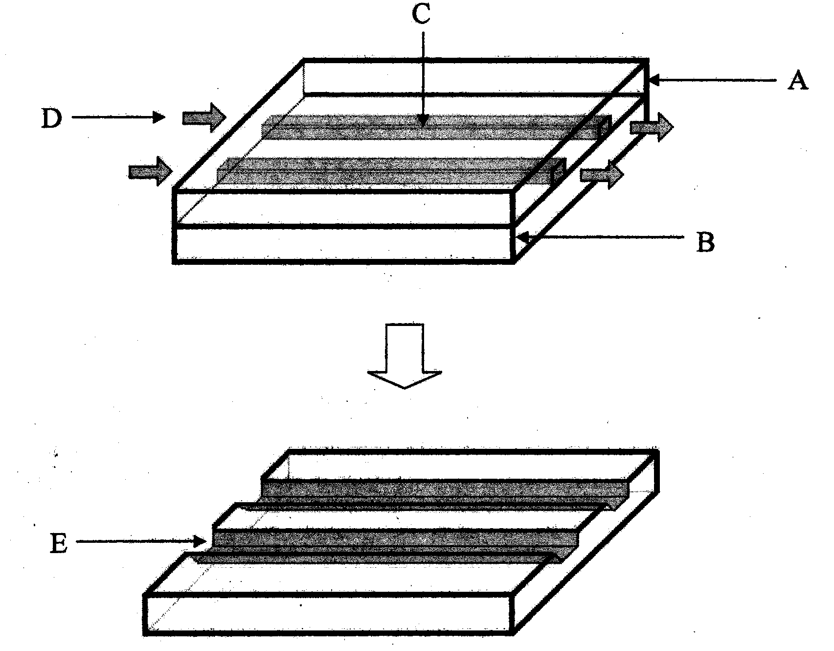
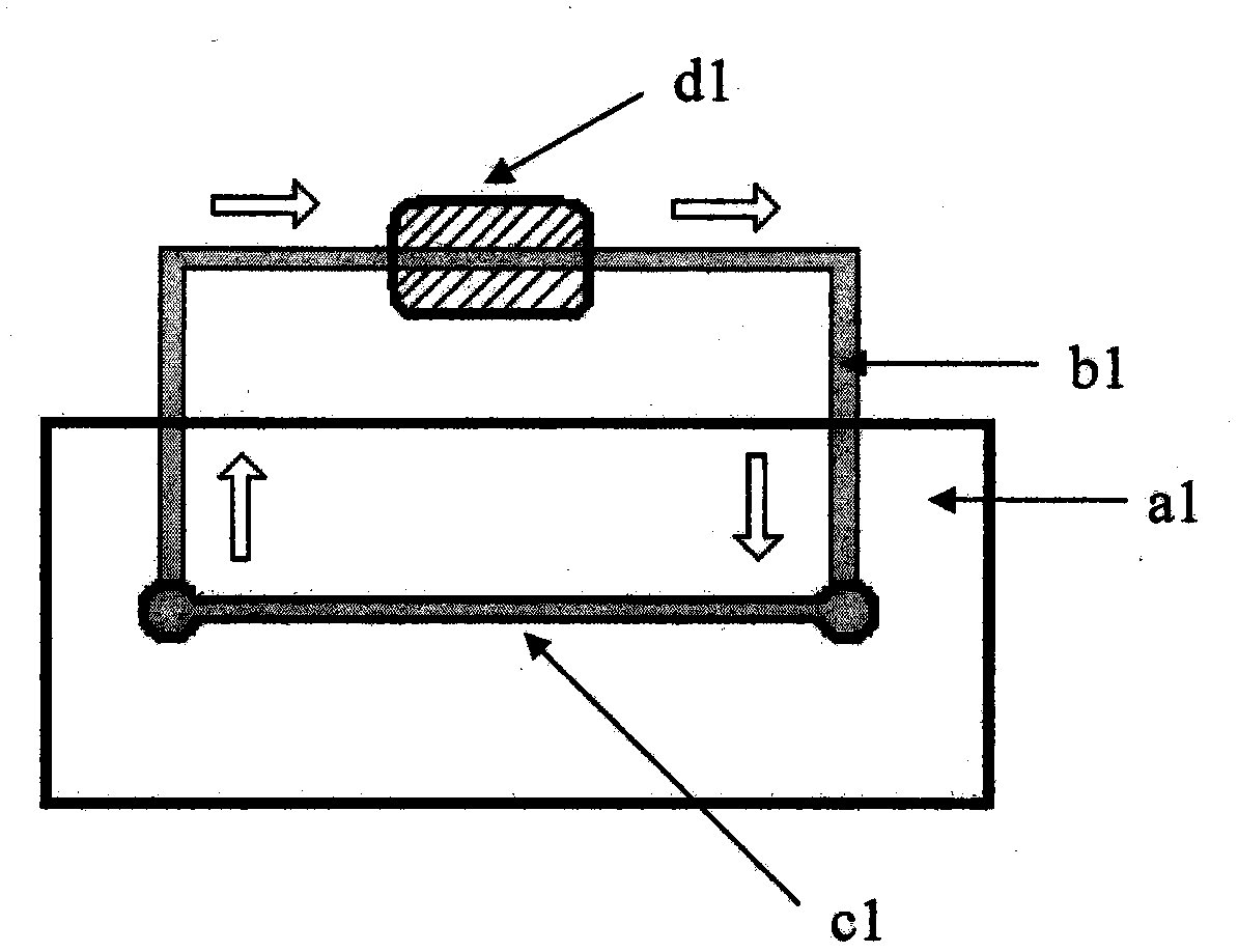
[0027] The structure and preparation method of a kind of criss-cross type glass microchannel are as Figure 4 shown. A PTFE cover sheet with a cross-shaped channel is closely attached to the glass substrate to be processed to form a chip a2 with a closed microchannel c2, and a peristaltic pump d2 is used to pump the hydrofluoric acid etching solution from the storage container e Draw out and inject into the inlet of the chip along the polytetrafluoroethylene hose b2, and the etching waste liquid is exported from the three outlets of the chip to the waste liquid storage container f. After etching for 20-30 minutes, the cover sheet and the base sheet are peeled off, and a cross-shaped microfluidic channel is obtained on the glass substrate. Using this system, the amount of etching solution can be reduced to a few milliliters level. Since the etching solution flows continuously from the surface to be etched,...

Embodiment 3

[0028] Embodiment 3 Preparation of a silicon substrate microchannel

[0029] The fabrication process of microchannels on silicon substrates is as follows: figure 1 As shown, the specific preparation process is as follows: firstly, the microchannel structure is processed on a smooth and flat polytetrafluoroethylene substrate by using precision numerical control CNC engraving technology, and then the substrate and the surface of the polished silicon wafer to be processed are reversibly bonded. combine( figure 1 a); Then use the external peristaltic pump system to continuously introduce the commercially available silicon etching solution into the microchannel along the polytetrafluoroethylene hose ( figure 1 b); the silicon etchant etches the area where the microchannel on the silicon wafer is to the required depth ( figure 1 c); Finally, the polytetrafluoroethylene substrate is peeled off from the surface of the silicon wafer to obtain a silicon substrate microchannel.


PUM

PropertyMeasurementUnit
depthaaaaaaaaaa

Abstract

The invention provides a manufacturing method of a micro-fluid channel. According to an adopted technical scheme, the manufacturing method comprises the following steps of adhering a substrate with a micro-channel structure to a substrate surface to be processed; and then continuously introducing an etching solution to the substrate surface by virtue of an external pump valve system so as to realize rapid processing of the micro-fluid channel. By using the manufacturing method of the micro-fluid channel provided by the invention, a manufacturing process is rapid and simple, an etching sacrificial layer does not need to be prepared, the usage amount of the etching solution is greatly reduced, meanwhile the etching efficiency is remarkably improved; the manufacturing method is especially suitable for rapidly manufacturing micro-fluidic chips with low cost and slight pollution on a large scale.

Description

technical field [0001] The invention relates to the field of micromachining, in particular to a manufacturing method of a microfluidic channel. Background technique [0002] Microfluidic chip is a kind of miniature reaction or analysis system characterized by microchannel network. Due to the advantages of fast analysis speed, low reagent consumption, low cost of use, easy integration and automation, microfluidic chips have been widely used in research in the fields of chemistry, biology, and medicine. [0003] At present, the materials used to make microfluidic chips mainly include inorganic materials such as silicon, glass, quartz, and metal, as well as organic polymers such as polymethyl methacrylate (PMMA) and polydimethylsiloxane (PDMS). All kinds of materials have their own characteristics and are suitable for different fields. The manufacturing process of microfluidic chips mainly includes microchannel preparation and chip bonding. The existing microchannel preparati...

Claims


Application Information

Patent Timeline
Patent Type & Authority Applications(China)
IPC IPC(8): B81C1/00
Inventor 叶嘉明吕志荣苑宝龙牟航
Owner XIAOSHAN BIOENG CENT OF YANGTZE DELTA REGION INST OF TSINGHUA UNIV ZHEJIANG
Why Eureka
Try Eureka