Organic light-emitting device and preparation method thereof
An electroluminescent device and luminescent technology, which is applied in the direction of electric solid-state devices, semiconductor/solid-state device manufacturing, electrical components, etc., to achieve the effects of improving light transmittance, cheap materials, and excellent packaging effects
- Summary
- Abstract
- Description
- Claims
- Application Information
AI Technical Summary
Problems solved by technology
Method used
Image

Examples
Embodiment 1
[0055] A method for preparing an organic electroluminescent device, comprising the following steps:
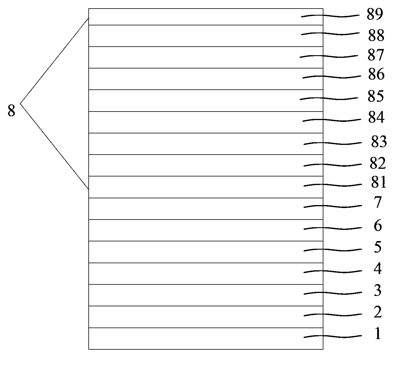
[0056] (1) Pre-treatment of ITO glass substrate 1: cleaning with acetone→cleaning with ethanol→cleaning with deionized water→cleaning with ethanol, all of which are cleaned with an ultrasonic cleaner for 5 minutes in a single wash, then blown dry with nitrogen, and dried in an oven for later use; Carry out surface activation treatment to the cleaned ITO glass substrate 1 to increase the oxygen content of the conductive surface layer and improve the work function of the conductive layer surface; the thickness of ITO is 100nm;
[0057] (2) Preparation of functional layer and light-emitting layer:
[0058] Hole injection layer 2: Evaporated MoO on ITO glass 1 3 Hybrid material obtained by doping NPB, MoO 3 The doping mass fraction is 30%, and the evaporation is carried out by high-vacuum coating equipment, and the vacuum degree during evaporation is 1×10 -5 Pa, the evaporation...
Embodiment 2
[0071] A method for preparing an organic electroluminescent device, comprising the following steps:
[0072] (1), (2), (3) are the same as embodiment 1;
[0073] (4) Preparation of organic barrier layer: CuPc was prepared on the cathode layer by vacuum evaporation, vacuum degree 5×10 -5 Pa, evaporation rate Thickness 250nm;
[0074] (5) Preparation of inorganic barrier layer: The inorganic barrier layer is prepared on the organic barrier layer by vacuum evaporation. The material of the inorganic barrier layer is a mixed material formed by a low refractive index material and a high refractive index material. The low refractive index material is MgF 2 , high refractive index materials are ZnSe, MgF 2 The mass fraction of the entire film layer is 60%, and the vacuum degree is 5×10 -5 Pa, evaporation rate Thickness 100nm;
[0075] (6) After step (5), use the same method and material as step (4) to prepare an inorganic barrier layer, and then use the same method and materi...
Embodiment 3
[0079] A method for preparing an organic electroluminescent device, comprising the following steps:
[0080] (1), (2), (3) are the same as embodiment 1;
[0081] (4) Preparation of organic barrier layer: NPB was prepared on the cathode layer by vacuum evaporation with a vacuum degree of 5×10 -5 Pa, evaporation rate Thickness 200nm;
[0082] (5) Preparation of inorganic barrier layer: The inorganic barrier layer is prepared on the organic barrier layer by vacuum evaporation. The material of the inorganic barrier layer is a mixed material formed by a low refractive index material and a high refractive index material. The low refractive index material is LiF, the high refractive index material is CdS, LiF accounts for 50% of the mass fraction of the entire film, and the vacuum degree is 5×10 -5 Pa, evaporation rate Thickness 150nm;
[0083] (6) After step (5), use the same method and material as step (4) to prepare an inorganic barrier layer, and then use the same method a...
PUM
| Property | Measurement | Unit |
|---|---|---|
| Water oxygen permeability | aaaaa | aaaaa |
| Water oxygen permeability | aaaaa | aaaaa |
| Water oxygen permeability | aaaaa | aaaaa |
Abstract
Description
Claims
Application Information
 - R&D
- Intellectual Property
- Life Sciences
- Materials
- Tech Scout
- Unparalleled Data Quality
- Higher Quality Content
- 60% Fewer Hallucinations
Browse by: Latest US Patents, China's latest patents, Technical Efficacy Thesaurus, Application Domain, Technology Topic, Popular Technical Reports.
© 2025 PatSnap. All rights reserved.Legal|Privacy policy|Modern Slavery Act Transparency Statement|Sitemap|About US| Contact US: help@patsnap.com