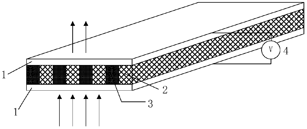
Voltage-modulated periodic subwavelength metal grating filter and preparation method thereof
A technology of metal grating and voltage modulation, applied in diffraction grating, nonlinear optics, optics, etc., can solve the problems affecting the high integration and multi-function of the system, and achieve the effect of easy implementation and simple process
- Summary
- Abstract
- Description
- Claims
- Application Information
AI Technical Summary
Problems solved by technology
Method used
Image
Examples
preparation example Construction
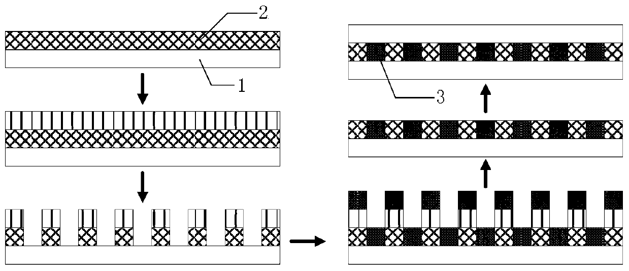
[0025] Such as image 3 Shown is a method for preparing a voltage-modulated periodic sub-wavelength metal grating filter, including the following steps in sequence:
[0026] (1) On a layer of transparent conductive glass, use thermal evaporation or magnetron sputtering to prepare a layer of metal film, the thickness of the metal film is a, and the material of the metal film can be precious metal material or ordinary metal material;
[0027] (2) Spin-coat a layer of photoresist on the surface of the metal film and dry it, the thickness of the photoresist is b;
[0028] (3) Groove arrays are prepared by etching processes such as focused ion beams to form slits arranged in a periodic array, and the depth of the grooves is a+b;
[0029] (4) Coating a photoelectric crystal film on the surface of the groove array by using a coating process such as electron beam evaporation, and the thickness of the photoelectric crystal film is a;
[0030] (5) Use cleaning solution to clean and dr...
Embodiment 1
[0034] In order to realize a periodic sub-wavelength metal grating filter, potassium dihydrogen phosphate is selected as the filler. ITO transparent glass was selected as the substrate, and a layer of gold film with a thickness of 300nm was prepared on the surface by thermal evaporation, and a layer of photoresist with a thickness of 200nm was spin-coated on the surface of the gold film and dried. Use focused ion beam technology to etch a periodic rectangular groove array with a depth of 500nm, a width of 200nm, and a period of 500nm, and then use electron beam evaporation to coat a layer of potassium dihydrogen phosphate with a thickness of 300nm on the surface of the groove array, and then use The cleaning solution cleans off the photoresist in the structure, dries it, and finally covers the upper surface with an ITO transparent electrode. And connect the upper and lower electrodes to the voltage generator.
[0035] The incident light is incident from the ITO transparent el...
Embodiment 2
[0037] In order to realize a periodic sub-wavelength metal grating filter, lithium tantalate was selected as the grating slit filler, ITO transparent glass was selected as the substrate, and a silver film with a thickness of 250nm was prepared on the surface by magnetron sputtering. A layer of photoresist with a thickness of 150 nm was spin-coated on the surface of the silver film and dried. Use focused ion beam technology to etch a periodic rectangular groove array with a depth of 400nm, a width of 250nm, and a period of 400nm, and then use electron beam evaporation to coat a layer of lithium tantalate with a thickness of 250nm on the surface of the groove array, and then use cleaning Clean the photoresist in the structure with liquid, dry it, and finally cover the upper surface with ITO transparent electrodes. And connect the upper and lower electrodes to the voltage generator.
[0038] The incident light is incident from the ITO transparent electrode below the filter, and ...
PUM
| Property | Measurement | Unit |
|---|---|---|
| Thickness | aaaaa | aaaaa |
| Width | aaaaa | aaaaa |
| Thickness | aaaaa | aaaaa |
Abstract
Description
Claims
Application Information


