Method for growing gate dielectric on gallium nitride substrate and electrical performance testing method

A gallium nitride substrate and testing method technology, applied in semiconductor/solid-state device testing/measurement, circuits, electrical components, etc., can solve the problems of large influence of gate capacitance, reduction of gate capacitance, unfavorable device application, etc.

Active Publication Date: 2014-04-23
SHANGHAI SIMGUI TECH
View PDF3 Cites 3 Cited by
  • Summary
  • Abstract
  • Description
  • Claims
  • Application Information

AI Technical Summary

Problems solved by technology

Although there is no urgent requirement for gate dielectric thickness in the manufacture of MIS-HEMT devices like silicon CMOS devices, the advantages of using high-K gate dielectrics on GaN are also obvious. Exhaust type devices are mainly used, so the threshold voltage is negative, and if a dielectric layer is added, the threshold voltage negative

Method used


Image

  • Method for growing gate dielectric on gallium nitride substrate and electrical performance testing method
  • Method for growing gate dielectric on gallium nitride substrate and electrical performance testing method
  • Method for growing gate dielectric on gallium nitride substrate and electrical performance testing method

Examples


Embodiment Construction

[0023] The specific implementation of the method for growing a gate dielectric on a GaN substrate and the method for testing electrical properties provided by the present invention will be described in detail below with reference to the accompanying drawings.

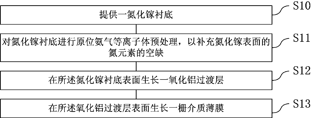
[0024] attached figure 1 Shown is a flowchart of the steps of the method for growing a gate dielectric on a gallium nitride substrate according to the present invention. The method includes the following steps: step S10, providing a gallium nitride substrate; step S11, performing an original process on the gallium nitride substrate Ammonia gas plasma pretreatment to supplement the vacancy of nitrogen element on the surface of gallium nitride; step S12, growing an aluminum oxide transition layer on the surface of the gallium nitride substrate; step S13, growing an aluminum oxide transition layer on the surface of the gallium nitride gate dielectric film.

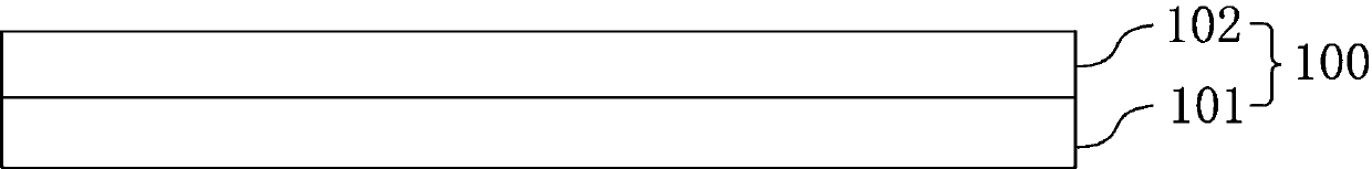
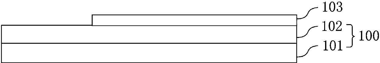
[0025] attached Figure 2A ~ attached Figure 2C Shown is a pr...


PUM


Abstract

The invention provides a method for growing gate dielectric on a gallium nitride substrate and an electrical performance testing method. The method for growing gate dielectric on the gallium nitride substrate comprises the steps of providing the gallium nitride substrate; performing in-situ ammonia plasma pretreatment to the gallium nitride substrate to compensate nitrogen onto the surface of gallium nitride; growing an aluminum oxide transition layer on the surface of the gallium nitride substrate; growing a gate dielectric thin film on the surface of the aluminum oxide transition layer. The method for growing gate dielectric on the gallium nitride substrate and the electrical performance testing method provided by the invention has the advantages that the high-quality gate dielectric can be grown on the gallium nitride substrate and the electrical performance of the gate dielectric can be simply and conveniently tested.

Description

technical field [0001] The invention relates to the technical field of integrated circuits, in particular to a method for growing a gate dielectric on a gallium nitride substrate and an electrical performance testing method. Background technique [0002] Semiconductor materials are key basic materials for the production of electronic components such as integrated circuits, transistors, power electronic devices, and semiconductor optoelectronic devices. They support the development of electronic information industries such as communications, computers, and network technologies, and are known as the food of electronic information. In the development of semiconductors, silicon and germanium are generally called the first-generation semiconductor materials; gallium arsenide, gallium phosphide, indium phosphide, aluminum arsenide and their alloys are the second-generation semiconductor materials; Wide-bandgap semiconductor materials with a width greater than 2.3ev, such as galliu...

Claims


Application Information

Patent Timeline
IPC IPC(8): H01L21/28H01L21/283H01L21/66
CPCH01L21/28264H01L21/285H01L22/14
Inventor 魏星曹铎狄增峰方子韦
Owner SHANGHAI SIMGUI TECH
Why Eureka
Try Eureka