A method for etching extremely-thin electrical isolation grooves on the surface of an ITO conductive thin film

A conductive thin film, surface etching technology, applied in circuits, photovoltaic power generation, electrical components, etc., can solve the problems of difficult to reach 50μm micro groove width, poor processing quality and efficiency, low groove speed, etc., to improve the utilization of materials. efficiency, improved battery performance, high processing efficiency

Active Publication Date: 2014-04-23
XI AN JIAOTONG UNIV
View PDF4 Cites 47 Cited by
  • Summary
  • Abstract
  • Description
  • Claims
  • Application Information

AI Technical Summary

Problems solved by technology

Since the nanosecond pulse width is much longer than the thermal diffusion time of the material, during the ablation removal process of the material, it is affected by heat conduction, causing serious thermal impact and thermal damage to the edge state of the active area
When processing nanosecond laser ablation processing with a thin-film solar cell groove structure, there are many problems, such as protrusions on the edge of the processed micro-groove, shunt or short circuit from the local to the upper layer; Micro-cracks and local material peeling, thereby shortening the service life of solar cells; when the laser pulse superposition rate is too high, due to th

Method used


Image

  • A method for etching extremely-thin electrical isolation grooves on the surface of an ITO conductive thin film
  • A method for etching extremely-thin electrical isolation grooves on the surface of an ITO conductive thin film
  • A method for etching extremely-thin electrical isolation grooves on the surface of an ITO conductive thin film

Examples


Embodiment 1

[0020] A method for etching extremely fine electrical isolation grooves on the surface of an ITO conductive film includes the following steps:

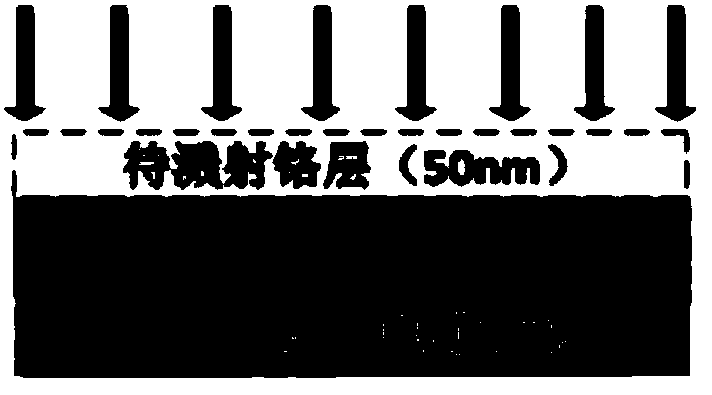
[0021] 1) First, sputter 50nm thick metallic chromium on the reverse side of the ITO conductive film glass substrate, such as figure 1 Shown

[0022] 2) Secondly, fix the ITO conductive film glass substrate on the stage, with the metal chromium side on the side of the laser emitting area, and keep the area of ​​the ITO conductive film side that needs to be grooved not to touch the stage;

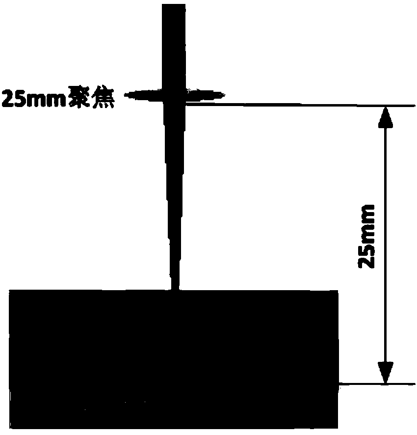
[0023] 3) Finally, using a picosecond laser with a wavelength of 532nm, a repetition frequency of 1KHz, a pulse width of 10ps, and a power of 12mw, a focusing lens with a focal length of 25mm is used to back-etch the ITO conductive film at a speed of 0.3mm / s, and the skin The center line of the second laser beam must be perpendicular to the surface of the ITO conductive film, and the focus position must be maintained on the ITO conductive film layer during...

Embodiment 2

[0025] A method for etching extremely fine electrical isolation grooves on the surface of an ITO conductive film includes the following steps:

[0026] 1) First, sputter 50nm thick metallic chromium on the reverse side of the ITO conductive film glass substrate, such as figure 1 Shown

[0027] 2) Secondly, fix the ITO conductive film glass substrate on the stage, with the metal chromium side on the side of the laser emitting area, and keep the area of ​​the ITO conductive film side that needs to be grooved away from the stage;

[0028] 3) Finally, use a picosecond laser with a wavelength of 532nm, a repetition frequency of 1KHz, a pulse width of 10ps, and a power of 10mw, and use a lens with a focal length of 25mm to focus, and back-etch the ITO conductive film at a speed of 0.4mm / s, and The center line of the picosecond laser beam must be perpendicular to the surface of the ITO conductive film, and the focal position must be kept on the ITO conductive film layer during the entire pr...

Embodiment 3

[0030] A method for etching extremely fine electrical isolation grooves on the surface of an ITO conductive film includes the following steps:

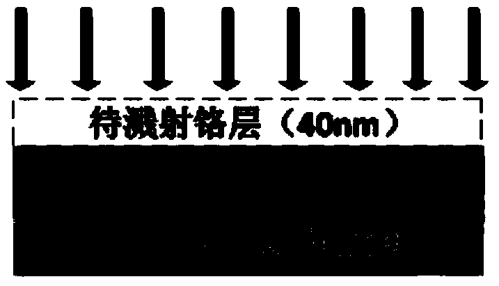
[0031] 1) First, sputter 40nm thick metallic chromium on the reverse side of the ITO conductive film glass substrate, such as image 3 Shown

[0032] 2) Secondly, fix the ITO conductive film glass substrate on the stage, with the metal chromium side on the side of the laser emitting area, and keep the area of ​​the ITO conductive film side that needs to be grooved away from the stage;

[0033] 3) Finally, using a picosecond laser with a wavelength of 532nm, a repetition frequency of 1KHz, a pulse width of 10ps, and a power of 12mw, a focus lens with a focal length of 25mm, and a scanning speed of 0.3mm / s for backward etching of the ITO conductive film, and The center line of the picosecond laser beam must be perpendicular to the surface of the ITO conductive film, and the focal position must be kept on the ITO conductive film layer during th...


PUM


Abstract

The invention provides a method for etching extremely-thin electrical isolation grooves on the surface of an ITO conductive thin film. The method is characterized in that, to begin with, sputtering metal chromium on the reverse side of an ITO conductive thin film glass substrate; fixing the ITO conductive thin film glass substrate on an object bearing table, with the side having the metal chromium being on the side of laser emission area and keeping the area needing etching on one side of the ITO conductive thin film not to be contacted with the object bearing table; and at last, utilizing picoseconds laser to etch ITO conductive thin film backwardly, wherein the center line of the picoseconds laser beam must keep perpendicular to the surface of the ITO conductive thin film and the focal position of the picoseconds laser must be on the ITO conductive thin film in the whole processing process. The method in the invention effectively reduces the width of the grooves in the surface of the ITO conductive thin film in a thin-film solar cell, guarantees processing efficiency of the picoseconds laser, and improves the overall level of the thin-film solar cell manufacture.

Description

Technical field [0001] The invention belongs to the field of micro-manufacturing technology, and specifically relates to a method for etching extremely fine electrical isolation grooves on the surface of an ITO conductive film. Background technique [0002] At present, thin film technology is applied to the field of new solar cell manufacturing, successfully solving the high cost problem of crystalline silicon solar cells. Due to the high light transmittance in the visible light region and good conductivity, the ITO conductive film with electrical isolation grooves on the surface is widely used as the front surface electrode of thin film solar cells. In the manufacturing process of thin-film solar cells, it is usually necessary to cut the whole ITO film into several units by textured electrical isolation grooves, and through the structural design, a series structure is formed between each unit to achieve the best voltage and current ratio. The size and accuracy level of the elec...

Claims


Application Information

Patent Timeline
IPC IPC(8): H01L31/18
CPCH01L31/022425H01L31/022475H01L31/1888Y02E10/50Y02P70/50
Inventor 王文君刘鹏梅雪松王恪典刘斌赵万芹
Owner XI AN JIAOTONG UNIV
Why Eureka
Try Eureka