Back passivating method and preparation method of crystalline silicon solar cell

A technology for solar cells and crystalline silicon, applied in the field of solar cells, can solve the problems of poor passivation effect, high cost, and difficulty in increasing the back passivation process.

Inactive Publication Date: 2014-04-23
CSG PVTECH
View PDF5 Cites 5 Cited by
  • Summary
  • Abstract
  • Description
  • Claims
  • Application Information

AI Technical Summary

Problems solved by technology

The deposition method can only deposit a layer of passivation film on the back surface of the silicon wafer, and the front side is not affected. The process is simple and easy to integrate into the conventional production process, but the passivation effect is poor, the conversion efficiency of the battery cannot be greatly improved, and the cost is expens

Method used


Image

  • Back passivating method and preparation method of crystalline silicon solar cell

Examples


preparation example Construction

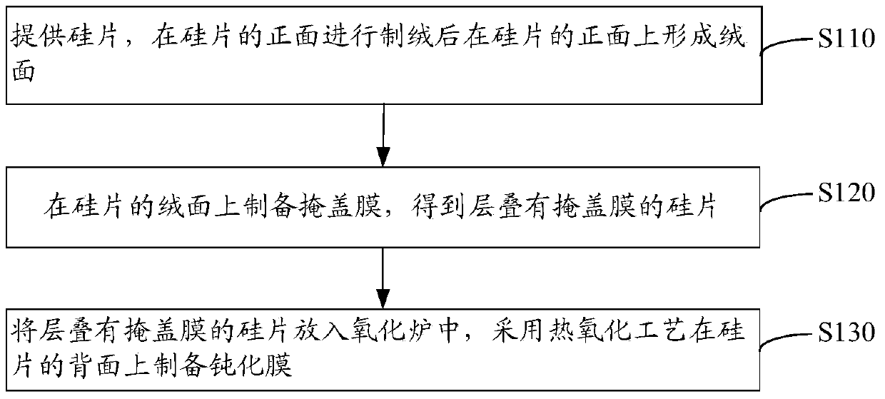
[0044] Further, a method for preparing a crystalline silicon solar cell is provided. The preparation method of the crystalline silicon solar cell includes the above step S110, step S120 and step S130, and also includes the following step S140.

[0045] Step S140: forming a positive electrode and a back electrode on the mask film and the passivation film respectively to obtain a crystalline silicon solar cell.

[0046] In one embodiment, the corrosive paste is first printed on the mask film by screen printing process, then placed at room temperature for 5 minutes, then ultrasonically cleaned for 2 minutes, and dried, and the back surface of the silicon wafer is cut out. Point contact pattern. After cleaning the sample, use the screen printing process to print the electrode paste on the masking film and the passivation film respectively, and sinter at 780 ° C to 810 ° C for 5 seconds to 10 seconds to form a positive electrode on the front side of the silicon wafer. A back elec...

Embodiment 1

[0052] Preparation of crystalline silicon solar cells

[0053] 1. Provide P-type monocrystalline silicon wafers, use acid method to make texture, and form a textured surface on the front side of P-type monocrystalline silicon wafers;

[0054] 2. Put the textured silicon wafer into a diffusion furnace, and carry out phosphorus diffusion at 860°C, and the square resistance of phosphorus diffused to the silicon wafer is 70Ω / □;

[0055] 3. Remove phosphosilicate glass with hydrofluoric acid, and perform edge etching by wet method;

[0056] 4. Coating a layer of silicon nitride film on the front side of the silicon wafer by plasma enhanced chemical vapor deposition method to obtain a silicon wafer laminated with a masking film, the thickness of the silicon nitride film is 80nm;

[0057] 5. Put the silicon wafer laminated with the mask film into the oxidation furnace, and use the wet oxygen thermal oxidation process to perform thermal oxidation at 800°C to form a silicon dioxide fi...

Embodiment 2

[0061] Preparation of crystalline silicon solar cells

[0062] 1. Provide P-type monocrystalline silicon wafers, use acid method to make texture, and form a textured surface on the front side of P-type monocrystalline silicon wafers;

[0063] 2. Put the textured silicon wafer into a diffusion furnace, and carry out phosphorus diffusion at 830°C, and the square resistance of phosphorus diffused to the silicon wafer is 60Ω / □;

[0064] 3. Remove phosphosilicate glass with hydrofluoric acid, and perform edge etching by wet method;

[0065] 4. Coating a layer of silicon nitride film on the front side of the silicon wafer by plasma enhanced chemical vapor deposition method to obtain a silicon wafer laminated with a masking film, the thickness of the silicon nitride film is 90nm;

[0066] 5. Put the silicon wafer laminated with the mask film into the oxidation furnace, and use the wet oxygen thermal oxidation process to perform thermal oxidation at 650°C to form a silicon dioxide fi...


PUM

PropertyMeasurementUnit
Thicknessaaaaaaaaaa
Thicknessaaaaaaaaaa
Sheet resistanceaaaaaaaaaa

Abstract

The invention relates to a back passivating method and a preparation method of a crystalline silicon solar cell. The back passivating method of the crystalline silicon solar cell comprises the steps of providing a silicon chip, and forming a suede surface on the front surface of the silicon chip after sueding the front surface of the silicon chip; preparing a covering film on the suede surface of the silicon chip, and obtaining the silicon chip which is laminated with the covering film; putting the silicon chip which is laminated with the covering film in an oxidation furnace, and preparing a passivating film on the back surface of the silicon chip by adopting a thermal oxidation technology. According to the back passivating method of the crystalline silicon solar cell, disclosed by the invention, the covering film physical property of the covering film is utilized, and the passivating film is prepared on the back surface of the silicon chip by adopting the thermal oxidation technology; the advantages of a deposition method and the thermal oxidation technology are integrated, the front surface of the silicon chip can not be influenced by a growing process of the passivating film on the back surface of the silicon chip, the difficulty of a back passivating technology is not increased, the technology is simpler, and the passivating effect is good.

Description

technical field [0001] The invention relates to the technical field of solar cells, in particular to a back passivation method for a crystalline silicon solar cell and a preparation method for a crystalline silicon solar cell. Background technique [0002] Improving cell conversion efficiency is the most urgent goal of crystalline silicon solar cells. The back passivation technology solves the problem of low long-wavelength photon response efficiency caused by the high recombination rate of the back surface of the silicon wafer, and can greatly improve the conversion efficiency of the cell, so it has become the focus of research and development in the industry and academia. [0003] At present, there are two main processes for manufacturing the back passivation structure: a passivation film is formed on the back surface of the silicon wafer by a deposition method (chemical vapor deposition or atomic layer deposition) or a thermal oxidation process. The deposition method can...

Claims


Application Information

Patent Timeline
IPC IPC(8): H01L31/18H01L31/0216
CPCH01L31/02167H01L31/068H01L31/1868Y02E10/547Y02P70/50
Inventor 廖辉梁杭伟祁嘉铭叶雄新孙小菩彭华罗静
Owner CSG PVTECH
Why Eureka
Try Eureka