An InGaN-based multi-quantum well structure and a method for preparing the same

A technology of quantum well and quantum well layer is applied in the field of InGaN-based multi-quantum well structure and its preparation, which can solve the problems of large half-height width of luminescence peak and uneven light wavelength, and achieves small half-height width, high luminous efficiency and emission The effect of uniform wavelength of light

Active Publication Date: 2014-04-23
TAIYUAN UNIV OF TECH
View PDF6 Cites 25 Cited by
  • Summary
  • Abstract
  • Description
  • Claims
  • Application Information

AI Technical Summary

Problems solved by technology

[0004] The technical problem to be solved by the present invention is that in the structure of the multi-quantum well light-emitting diode in the prior art, the light-emitting peak half-width ratio is relatively l

Method used


Image

  • An InGaN-based multi-quantum well structure and a method for preparing the same
  • An InGaN-based multi-quantum well structure and a method for preparing the same

Examples


Embodiment 1

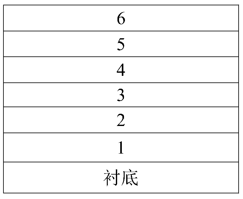
[0048] This embodiment provides a kind of LED structure, its structure is as follows figure 1 As shown, along the growth direction are sapphire substrate, low-temperature GaN nucleation layer, high-temperature undoped u-GaN layer, Si-doped n-GaN layer, the InGaN / GaN-based multiple quantum well structure, p- AlGaN electron blocking layer and Mg doped p-GaN layer.

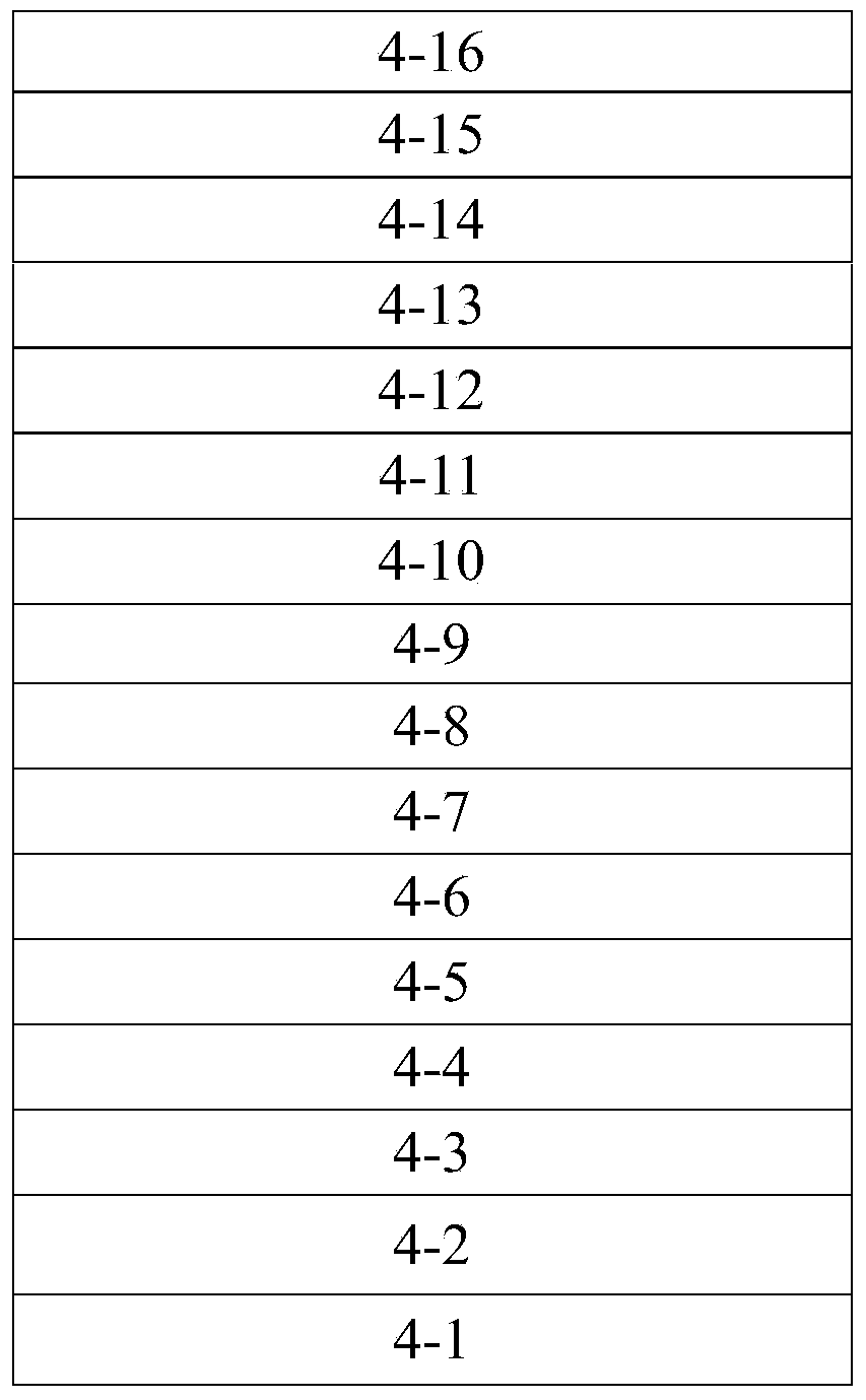
[0049] Wherein, the structure of the InGaN-based multiple quantum wells is as follows figure 2 As shown, along the growth direction, they are: the first GaN barrier layer, the first In composition incremental quantum well layer, the first Si-doped GaN barrier layer, the second In composition incremental quantum well layer, The second Si-doped GaN barrier layer, the third In composition incremental quantum well layer, the third Si-doped GaN barrier layer, the first fixed In composition quantum well layer, and the first In composition decreasing barrier layer layer, the second GaN barrier layer, the second quantum w...

Embodiment 2

[0078] This embodiment provides an LED structure, which includes a sapphire substrate, a low-temperature GaN nucleation layer, a high-temperature undoped u-GaN layer, a Si-doped n-GaN layer, and the InGaN / GaN-based multilayer Quantum well structure, p-AlGaN electron blocking layer and Mg doped p-GaN layer.

[0079] Wherein, the structure of the InGaN-based multiple quantum wells includes: along the growth direction, the first GaN barrier layer, the first In composition incremental quantum well layer, the first Si-doped GaN barrier layer, and the second In group Gradual quantum well layer, second Si-doped GaN barrier layer, third In composition gradual quantum well layer, third Si-doped GaN barrier layer, first fixed In composition quantum well layer , the first In composition decreasing barrier layer, the second GaN barrier layer, the second quantum well layer with fixed In composition, the second In composition reducing barrier layer, the third GaN barrier layer, the third qu...

Embodiment 3

[0108] This embodiment provides an LED structure, which includes a sapphire substrate, a low-temperature GaN nucleation layer, a high-temperature undoped u-GaN layer, a Si-doped n-GaN layer, and the InGaN / GaN-based multilayer Quantum well structure, p-AlGaN electron blocking layer and Mg doped p-GaN layer.

[0109] Wherein, the structure of the InGaN-based multiple quantum wells includes: along the growth direction, the first GaN barrier layer, the first In composition incremental quantum well layer, the first Si-doped GaN barrier layer, and the second In group Gradual quantum well layer, second Si-doped GaN barrier layer, third In composition gradual quantum well layer, third Si-doped GaN barrier layer, first fixed In composition quantum well layer , the first In composition decreasing barrier layer, the second GaN barrier layer, the second quantum well layer with fixed In composition, the second In composition reducing barrier layer, the third GaN barrier layer, the third qu...


PUM

PropertyMeasurementUnit
Thicknessaaaaaaaaaa
Thicknessaaaaaaaaaa
Thicknessaaaaaaaaaa

Abstract

The invention relates to an InGaN-based multi-quantum well structure. Multilayer structures in which In constituent gradual increase quantum well layers and Si-doped GaN barrier layers are arranged alternately are successively grown on a GaN barrier layer. Then, along a growth direction, multiplayer structures in which fixed-In-constituent quantum well layers, In constituent gradual decrease quantum well layers, and GaN barrier layers are arranged periodically are further grown. Therefore, the InGaN-based multi-quantum well structure may effectively alleviate stress at the interface between a barrier and a well and curving of an energy band, control a radiation recombination area of electrons and electron holes, increase the injection efficiency and the radiation recombination efficiency so as to be beneficial to further acquisition of a GaN-based LED structure with good crystal quality, high internal quantum efficiency, and high light-emitting efficiency. In addition, the light-emitting peak of the GaN-based LED structure has a low full width at half maximum and uniform wavelengths of emitted light.

Description

technical field [0001] The invention relates to an InGaN-based multi-quantum well structure and a preparation method thereof, belonging to the technical field of semiconductors. Background technique [0002] GaN-based light-emitting diodes (LEDs) can directly convert electrical energy into light energy, and the photoelectric conversion efficiency far exceeds that of traditional incandescent and fluorescent lamps. It can emit the entire wavelength band from ultraviolet to visible light, so it has a wide range of applications in indicator lights, backlights, displays, household and commercial lighting and other fields. However, in the epitaxially grown GaN-based LED structure, due to the bipolar input of carriers, electrons and holes are respectively concentrated in the quantum wells near the N-type doped region and the P-type doped region, causing the carrier In the uneven distribution between quantum wells, the overlap integral of the wave function of electrons and holes in...

Claims


Application Information

Patent Timeline
IPC IPC(8): H01L33/06H01L33/26H01L33/00
CPCH01L33/0066H01L33/0075H01L33/06H01L33/325
Inventor 贾伟党随虎许并社李天保梁建董海亮
Owner TAIYUAN UNIV OF TECH
Why Eureka
Try Eureka