Series boosting solar cell unit and manufacturing method thereof

A technology of solar cells and anode electrodes, applied in the field of solar energy, can solve problems such as difficulty in adapting to the development needs of miniaturization, inability to integrate electronic circuits on a single chip, and large overall system volume, so as to reduce system volume and cost, and avoid booster devices , The effect of simplifying the power supply system

Inactive Publication Date: 2014-04-30
TIANJIN UNIV
View PDF3 Cites 0 Cited by
  • Summary
  • Abstract
  • Description
  • Claims
  • Application Information

AI Technical Summary

Problems solved by technology

[0004] Although the self-supply of electronic system energy can be achieved by using conventional discrete solar cells, the conventional manufacturing process of solar cells makes it impossible to monolithically integrate with electronic circuits based on standard CMOS processes, so the overall system is large in size and high in cost. Adapt to the development needs of miniaturization

Method used


Image

  • Series boosting solar cell unit and manufacturing method thereof
  • Series boosting solar cell unit and manufacturing method thereof
  • Series boosting solar cell unit and manufacturing method thereof

Examples


Embodiment Construction

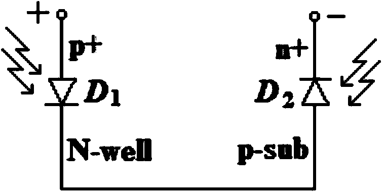
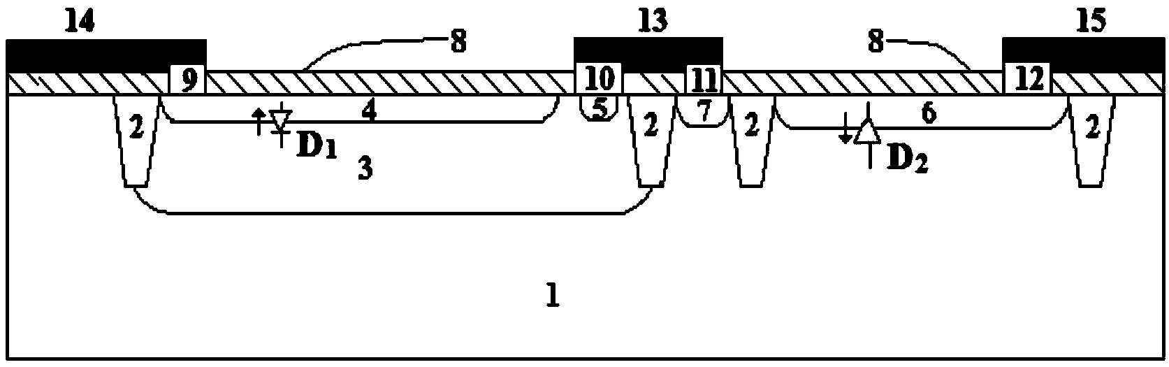
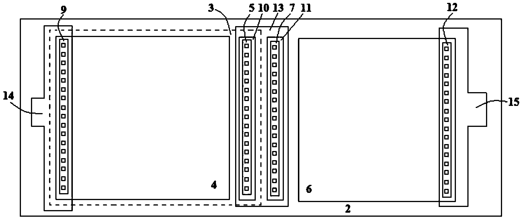
[0028]If the micro solar cell compatible with the standard CMOS process is monolithically integrated with the micro power consumption system chip, the on-chip power supply can be realized, the system volume and cost can be reduced, and the integration and function of the system can be continuously improved to realize the real self-power supply SoC.

[0029] In order to overcome the unfavorable factors such as the large volume and high cost of conventional solar cells, and realize the automatic energy acquisition of micro-power system chips that work periodically such as radio frequency identification and wireless sensor network nodes, the present invention proposes an on-chip integrated system compatible with standard CMOS technology. A series boost solar cell unit, which is expected to directly drive low-voltage, micro-power electronic systems such as radio frequency identification and wireless sensor network nodes.

[0030] The series boost solar cell unit proposed by the pr...


PUM

PropertyMeasurementUnit
Depthaaaaaaaaaa
Thicknessaaaaaaaaaa

Abstract

The invention belongs to the technical field of solar energy and provides a manufacturing method of a series boosting solar cell unit. According to the technical scheme, aiming to restrain electric charges generated by the SEE from diffusing in a chip, the method includes the following steps that firstly, shallow trench isolation areas are manufactured on a lightly-doped P- -type silicon substrate; secondly, an intermediately-doped N well is manufactured in a device active area between the shallow trench isolation areas; thirdly, a large-area heavily-doped P+ active area is manufactured on an N-type substrate through the ion implantation technology; fourthly, a heavily-doped N+ contact area is manufactured on the portion, outside the P+ active area, of the N-type substrate through the ion implantation technology; fifthly, a dielectric layer with a proper thickness is formed on the surface of a wafer in a deposition mode; sixthly, anodes and cathodes of two kinds of solar cells are manufactured on the upper surface of a device; seventhly, the anode and the cathode of the series boosting solar cell unit are manufactured. The method is mainly applied to design and manufacturing of the solar cells.

Description

technical field [0001] The invention belongs to the technical field of solar energy, and relates to a micro solar cell structure compatible with a complementary metal oxide semiconductor (CMOS) process; it relates to a series of standard CMOS process technologies such as oxidation, photolithography, etching, ion implantation, and metallization. The preparation method of the device, in particular, relates to a series boost solar cell unit and a preparation method thereof. Background technique [0002] With the deteriorating global ecological environment and the increasing shortage of traditional petrochemical energy, there is an urgent need for a clean, pollution-free and abundant new energy to promote the sustainable development of human civilization and social economy. one of the scientific problems. [0003] As the process nodes of integrated circuits continue to shrink, the operating voltage and power consumption of SoCs continue to decrease for microsystems that work pe...

Claims


Application Information

Patent Timeline
IPC IPC(8): H01L27/142H01L31/0352H01L31/18
CPCY02E10/50Y02P70/50
Inventor 谢生毛陆虹张世林侯贺刚
Owner TIANJIN UNIV
Why Eureka
Try Eureka