

Photoelectric printed board and manufacturing method thereof
A production method and printed board technology, applied in the direction of circuit substrate materials, multi-layer circuit manufacturing, printed circuit components, etc., can solve the problems of complex electrical interconnection conduction, complex assembly, difficult materials, etc., and achieve interconnection density High, simple manufacturing process, and simplified process steps
- Summary
- Abstract
- Description
- Claims
- Application Information
AI Technical Summary
Problems solved by technology
Method used
Image

Examples
Embodiment Construction
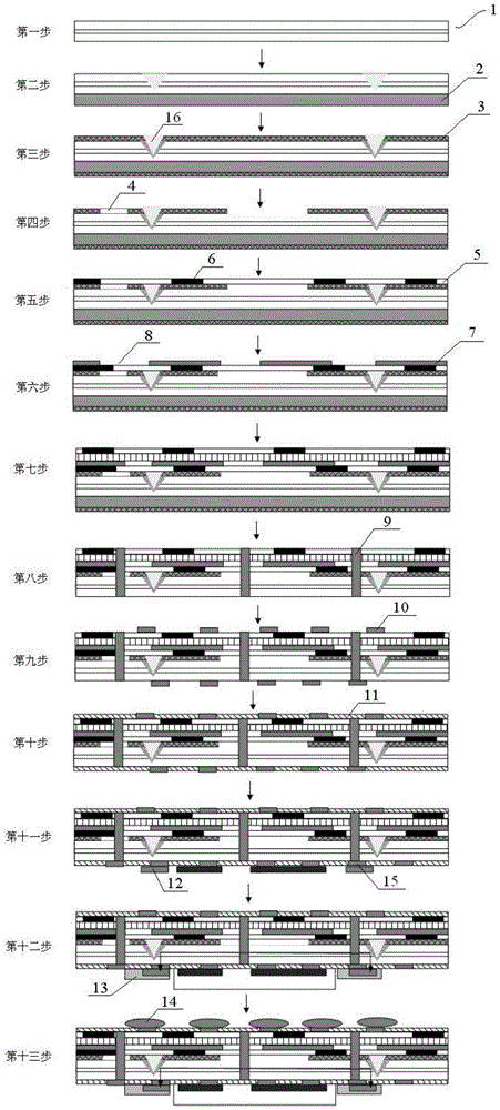
[0029] The present invention will be further described in detail below in conjunction with the accompanying drawings and specific embodiments.
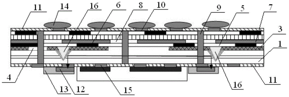
[0030] A kind of photoelectric printed board, its structure is as figure 1 As shown, it includes an optical waveguide layer 1, a first metal layer 3, a prepreg PP, and a second thick copper layer 7 arranged sequentially from bottom to top. layer 15 and metal protection layer 11, and the upper end surface of the second thick copper layer is provided with an upper outer copper layer 10 and a metal protection layer 11 that are fused together.
[0031] The optical waveguide layer 1 is provided with a reflector 16, the first metal layer 3 is provided with a pattern RDL1 communicating with the reflector, the prepreg PP is provided with a blind buried hole 6, and the second thick copper layer 7 is provided with a pattern RDL2 ; The through hole 9 runs through the optical waveguide layer 1 , the first metal layer 3 , the prepreg PP and the s...
PUM
 Abstract
Description
Claims
Application Information