Manufacturing method of transient voltage suppressor chip having tunneling effect

A technology of transient suppression and tunnel effect, which is applied in semiconductor/solid-state device manufacturing, electrical components, circuits, etc., can solve the problem of low withstand voltage, achieve the effect of reducing Vc value and realizing tunnel effect

Inactive Publication Date: 2014-05-07
上海瞬雷电子科技有限公司
View PDF3 Cites 13 Cited by
  • Summary
  • Abstract
  • Description
  • Claims
  • Application Information

AI Technical Summary

Problems solved by technology

Under normal circumstances, the VC value of TVS is about 1.3 times that of VBR. Although it can meet the device application of conventional solutions, with the vigorous development of semiconductor technology, the integrat

Method used


Image

  • Manufacturing method of transient voltage suppressor chip having tunneling effect
  • Manufacturing method of transient voltage suppressor chip having tunneling effect
  • Manufacturing method of transient voltage suppressor chip having tunneling effect

Examples


Embodiment Construction

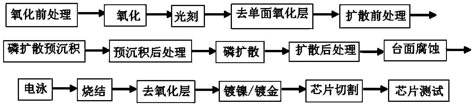
[0029] The technical solution of the present invention will be described in further detail below through specific embodiments in conjunction with the accompanying drawings.

[0030] Please refer to figure 1 , the flow chart of the method for manufacturing a chip with tunnel effect characteristics disclosed by the present invention mainly includes the following steps:

[0031] 1) Pre-oxidation treatment:

[0032] Chemically treat the surface of silicon wafers through electronic cleaning agents, deionized water cleaning and other processes;

[0033] 2) Oxidation:

[0034] Clean the original silicon wafer, and grow a layer of oxide layer as a mask in an oxidation furnace at 1100-1200 ° C to prevent the boron diffusion source from entering the N+ surface and groove;

[0035] 3) Photolithography:

[0036] Apply glue, expose, and develop the oxidized silicon wafer to form a mesa pattern;

[0037] 4) Remove the oxide layer on one side:

[0038] Remove the oxide layer on one sid...


PUM


Abstract

The invention discloses a manufacturing method of a transient voltage suppressor chip having the tunneling effect. The method comprises the following steps: 1) treatment before oxidation; 2) oxidation; 3) photoetching; 4) single-sided oxide layer removal; 5) treatment before diffusion; 6) phosphorus diffusion pre-deposition; 7) treatment after pre-deposition; 8) phosphorus diffusion; 9) treatment after diffusion; 10) mesa etching; 11) electrophoresis; 12) sintering; 13) oxide layer removal; 14) nickel plating and gold plating; 15) and chip cutting. The manufacturing method disclosed in the invention can be used to realize the tunneling effect of the chip to reduce the chip Vc value, wherein the Ipp capability of the chip is greater than a same conventional chip.

Description

technical field [0001] The invention relates to a chip, in particular to a manufacturing method of a transient suppression diode chip with tunnel effect. Background technique [0002] A transient diode (TVS) is a high-efficiency protection device in the form of a diode. When the two poles of the TVS diode are impacted by reverse transient high energy, it can change the high impedance between its two poles to low impedance at a speed of 10 minus 12 seconds, absorbing up to several thousand watts of surge power , while clamping the voltage at a predetermined value, effectively protecting the precision components in the electronic circuit from being damaged by various surge pulses. Because it has the advantages of fast response speed, large transient power, low leakage current, small breakdown voltage deviation, easy control of clamping voltage, no damage limit, small size, etc., it has been widely used in computer systems, communication equipment, communication equipment, etc...

Claims


Application Information

Patent Timeline
IPC IPC(8): H01L21/329
CPCH01L21/228H01L29/66098
Inventor 茅寅松盛锋
Owner 上海瞬雷电子科技有限公司
Why Eureka
Try Eureka