A kind of preparation method of semiconductor device

A semiconductor and device technology, applied in the field of semiconductor device preparation, can solve the problems of accelerating short channel effect, device performance degradation, boron diffusion, etc., and achieve the effect of eliminating short channel effect, good performance and reducing junction leakage

Active Publication Date: 2016-09-21
SEMICON MFG INT (SHANGHAI) CORP
View PDF6 Cites 0 Cited by
  • Summary
  • Abstract
  • Description
  • Claims
  • Application Information

AI Technical Summary

Problems solved by technology

[0003] In order to obtain better performance, in the process of preparing PMOS, epitaxial SiGe is usually carried out in the source and drain regions of PMOS to apply compressive stress to the channel of the substrate, and then ion implantation is performed after epitaxial SiGe to obtain a higher doping concentration. In this process, high-energy, low-dose B (Boron) is usually used to dope its source and drain to form a doping tail profile to reduce the leakage at the junction, or to perform epitaxial growth of SiGe At the same time, B (Boron) doping is performed on the source and drain, and the gas flow rate and other parameters are adjusted to achieve sufficient doping concentration. However, after ion implantation or in-situ doping on the source and drain of PMOS SiGe It usually leads to strain relaxation of the device after annealing, and the strain relaxation will directly lead to the degradation of device performance
[0004] At the same time, the SiGe epitaxy or deposition method in the prior art is to directly deposit a SiGeB layer with a certain concentration gradient without providing SiGe crystal grains to reduce junction leakage current, but the SiGeB layer with a certain concentration gradient will cause boron Diffusion into channels and accelerated short channel effects
Secondary ion mass spectroscopy (SIMS) on the device obtained by the existing method found that the concentration of the in-situ doped boron concentration in the channel of the device is too high, so it is easy to accelerate the short channel effect
[0005] Therefore, in order to reduce the source-drain relaxation caused by ion implantation, the source-drain implantation step should be skipped as much as possible, but the control of B distribution at the junction becomes a challenge, and it is necessary to improve the current source-drain implantation method in PMOS, and at the same time eliminate Accelerated short channel effects in the presence of

Method used


Image

  • A kind of preparation method of semiconductor device
  • A kind of preparation method of semiconductor device
  • A kind of preparation method of semiconductor device

Examples


Embodiment Construction

[0036] In the following description, a lot of specific details are given in order to provide a more thorough understanding of the present invention. However, it is obvious to those skilled in the art that the present invention can be implemented without one or more of these details. In other examples, in order to avoid confusion with the present invention, some technical features known in the art are not described.

[0037] In order to thoroughly understand the present invention, a detailed description will be provided in the following description to illustrate the manufacturing method of the semiconductor device of the present invention. Obviously, the implementation of the present invention is not limited to the specific details familiar to those skilled in the semiconductor field. The preferred embodiments of the present invention are described in detail as follows. However, in addition to these detailed descriptions, the present invention may also have other embodiments.

[0...


PUM


Abstract

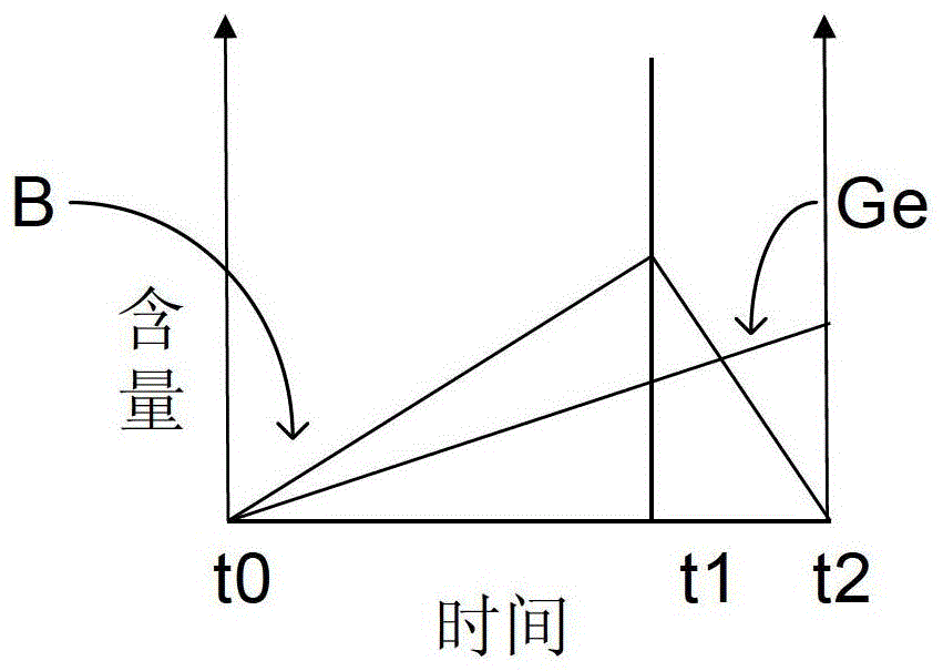
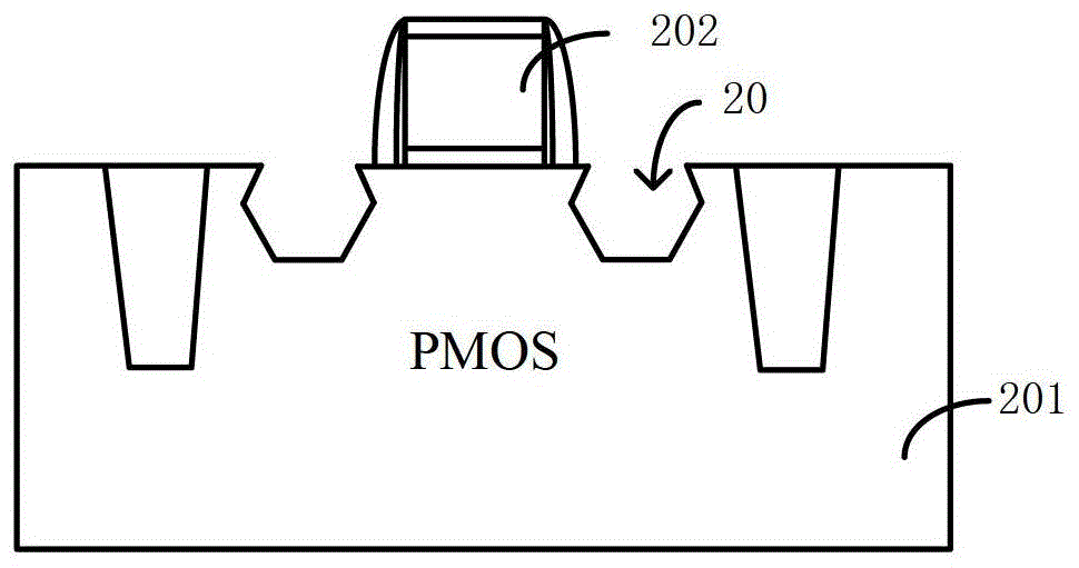
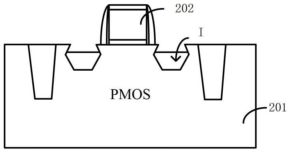
The invention relates to a semiconductor device preparing method. The method comprises the following steps: a semiconductor substrate is provided, wherein the semiconductor substrate at least includes a gate structure; and grooves are formed in two sides of the gate and a SiGeB layer is grown in the grooves through epitaxial growth. The method is characterized in that B is doped in an in-situ manner while performing the epitaxial growth of the SiGe layer, and the epitaxial growth comprises two stages: the first stage is to increase the concentration of B in the SiGe layer to make the concentration of B in the SiGe layer reaches the peak concentration; and the second stage is to reduce the concentration of B in the SiGe layer so as to eliminate the short-channel effect. Through the method of the invention, not only a more flat doping tail contour can be acquired after the B doping process is performed so as to reduce the junction leakage phenomenon, and the method can skip the separate ion implantation process so as to make the stress in the channel region maintained; and but also the method can be used to make the doping concentration of B at channels is low so as to eliminate the short-channel effect to make prepared devices have good performances.

Description

Technical field [0001] The present invention relates to the field of semiconductors. Specifically, the present invention relates to a method for manufacturing a semiconductor device. Background technique [0002] With the continuous development of semiconductor technology, the preparation of semiconductor devices tends to be miniaturized, and has now developed to the nanometer level, while the preparation process of conventional devices has gradually matured. The current method of preparing PMOS often includes the following conventional steps: first, a semiconductor substrate is provided, and then a double well, shallow trench isolation, and polysilicon gate structure are formed on the semiconductor substrate. As the width of the gate continues to decrease, the gate The channel length under the structure is also continuously reduced. In order to effectively prevent the short channel effect, a lightly doped drain process (LDD) is introduced in the integrated circuit manufacturing ...

Claims


Application Information

Patent Timeline
Patent Type & Authority Patents(China)
IPC IPC(8): H01L21/336H01L21/20
CPCH01L21/02381H01L21/02532H01L21/02579H01L21/0262H01L21/2053H01L29/165H01L29/66636H01L29/7848
Inventor 金兰涂火金何有丰
Owner SEMICON MFG INT (SHANGHAI) CORP
Why Eureka
Try Eureka