Wind power friction nanometer generator

A technology of nanometer generators and wind power generators, applied in the direction of friction generators, etc., can solve the problems of wind power generators with complex structures and inability to meet the power supply requirements of microelectronic devices, and achieve simple structure, high compatibility, and increased contact charge density Effect

Active Publication Date: 2014-05-07
BEIJING INST OF NANOENERGY & NANOSYST
View PDF5 Cites 41 Cited by
  • Summary
  • Abstract
  • Description
  • Claims
  • Application Information

AI Technical Summary

Problems solved by technology

It can be seen that the structure of the entire wind turbine is very complicated, requiring many large components, which cannot meet the power supply requirements of microelectronic devices at all.

Method used


Image

  • Wind power friction nanometer generator
  • Wind power friction nanometer generator
  • Wind power friction nanometer generator

Examples


Embodiment 1

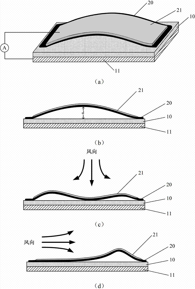
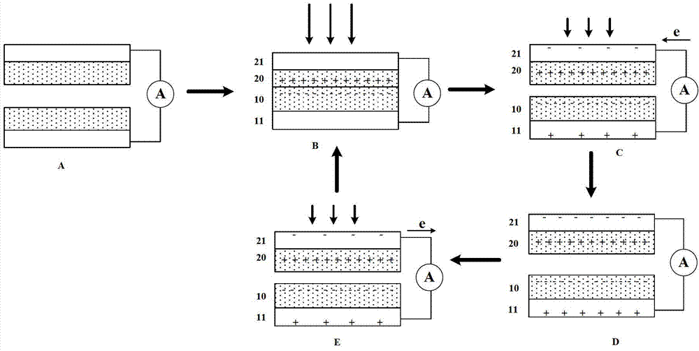
[0109] The first conductive element adopts a metal copper plate with a thickness of 1mm, and a layer of Teflon (polytetrafluoroethylene) film with a thickness of 25 microns is coated on it as the first friction layer, and the second friction layer and the second conductive element use Thickness is 40 μ m, long 5cm, wide 3cm metal aluminum thin film layer, the two ends of this thin film layer are fixed on the both sides of Teflon layer upper surface, make the formation height between metal aluminum layer and Teflon layer 2mm arch clearance. Connect the metal copper film layer and the metal aluminum layer to the external circuit through wires, and the blower provides airflow along the direction of the generator at a flow rate of about 5m / s. It can be clearly seen that the metal aluminum film layer vibrates, making it and the Teflon layer The contact-separation cycle is continuously formed between them, which can drive 80 commercial LED bulbs to emit light. For details, see Fig...

Embodiment 2

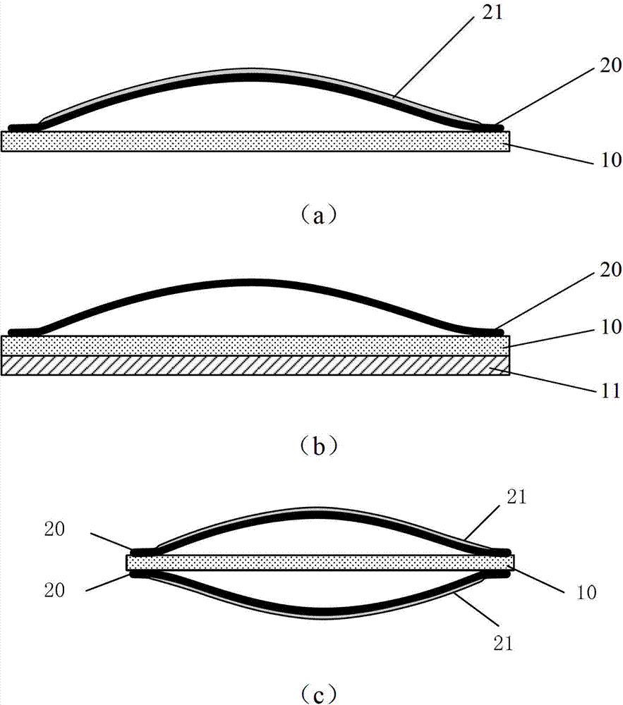
[0112] The first friction layer is made of Teflon (polytetrafluoroethylene) film, the first conductive element is made of metal copper film with a thickness of 200nm, and the first conductive element is deposited on the first friction layer by magnetron sputtering. The second friction layer and the second conductive element adopt a metal aluminum thin film layer with a thickness of 200nm, a length of 5cm, and a width of 2.5cm. The second friction layer and the second conductive element are deposited on a thickness of 25 μm by magnetron sputtering. on a polymer substrate. The substrate is a polyimide film, the length and width of which are consistent with the metal aluminum film layer. A plexiglass strip with a height of 2 mm, a length of 2.5 cm, and a width of 2 mm was prepared by laser cutting, and the strip was fixed on the upper surface of the Teflon layer. One end of the polyimide film deposited with the metal aluminum film layer is fixed on the upper surface of the strip...

Embodiment 3

[0114] Polydimethylsiloxane (English abbreviated as PDMS) with a thickness of 100 microns is used as the second friction layer, and a metal gold film with a thickness of about 100 nm is deposited on it by magnetron sputtering as the second friction layer. Conductive elements. A silicon wafer with a thickness of 500 μm is used as the first friction layer, and a metal silver film is deposited on its lower surface with a thickness of about 100 nm. The other side of the silicon wafer is spin-coated with a layer of photoresist, and a square window array with a side length of micron or sub-micron level is formed on the photoresist by photolithography; the silicon wafer after photolithography is completed After chemical etching with hot potassium hydroxide, a pyramid-shaped concave structure array is formed at the window. When the silicon wafer and PDMS are in contact with the two materials under the action of air flow, due to the good elasticity of PDMS, it can enter and fill the c...


PUM


Abstract

This invention provides a wind power friction nanometer generator comprising a first part and a second part which can perform elastic bending deformation. The first part comprises a first conducting element and a first friction layer which is directly attached to the upper surface of the first conducting element; the second part comprises a second friction layer and a second conducting element which is directly attached to the upper surface of the second friction layer; at least one of the first part and the second part is relatively fixed, and the first friction layer and the second friction layer are opposite to each other; at least part of the upper surface of the first friction layer and the lower surface of the second friction layer form a contact-separate circulation under the action of the wind force, and electric signals are outputted to an external circuit through the first conducting element and the second conducting element. When tangential periodic external forces are applied on the sliding friction nanometer generator, alternating current pulse signal output is formed between the first conducting element and the second conducting element.

Description

technical field [0001] The invention relates to a wind power generator, in particular to a nanometer generator which utilizes wind force to drive contact friction to generate electricity. Background technique [0002] With the rapid rise of the Internet of Things technology, a large number of new microelectronic devices with multiple functions and high integration have been continuously developed, and have shown unprecedented application prospects in various fields of people's daily life. However, the research on the power supply system matched with these microelectronic devices is relatively lagging behind. Generally speaking, the power supply of these microelectronic devices all comes from batteries directly or indirectly. Batteries are not only large in size and heavy in weight, but also contain toxic chemical substances that are potentially harmful to the environment and the human body. Therefore, it is of great significance to develop technologies that can convert natu...

Claims


Application Information

Patent Timeline
Patent Type & Authority Applications(China)
IPC IPC(8): H02N1/04
CPCH02N1/04
Inventor 王中林朱光林宗宏
Owner BEIJING INST OF NANOENERGY & NANOSYST
Why Eureka
Try Eureka