Preparation method of secondary-electron emission thin film

A secondary electron emission and thin film technology, which is applied in sputtering plating, ion implantation plating, vacuum evaporation plating, etc., can solve the problem of reducing the conductivity of the film, poor applicability of magnesium oxide film, and reducing the secondary electron emission of magnesium oxide Coefficient and other issues, to achieve the effect of flexible film forming process and easy control of thickness

Inactive Publication Date: 2014-05-14
XI AN JIAOTONG UNIV
View PDF3 Cites 13 Cited by
  • Summary
  • Abstract
  • Description
  • Claims
  • Application Information

AI Technical Summary

Problems solved by technology

However, the thickness of the MgO layer on the surface of the film prepared by this method is difficult to accurately control. If the surface MgO layer is too thick, the conductivity of the film will be reduced, thereby affecting the stability of secondary electron emission. If it is too thin, the secondary electrons of the film will be reduced. Emission coefficient
And, Ar + Sputtering treatment will cause damage to the surface magnesium oxide grains and reduce the secondary electron emission coefficient of magnesium oxide
especially since Ar + The difference in the sputtering rate of various metals and magnesium oxide is also different. Some metals have little difference in the sputtering rate of MgO due to their low sputtering rate or strong binding force with MgO. Use this method to prepare thin layers with high MgO content on the surface, so this method is less applicable to prepare MgO thin films doped with different metal materials

Method used


Image

  • Preparation method of secondary-electron emission thin film
  • Preparation method of secondary-electron emission thin film
  • Preparation method of secondary-electron emission thin film

Examples


Embodiment 1

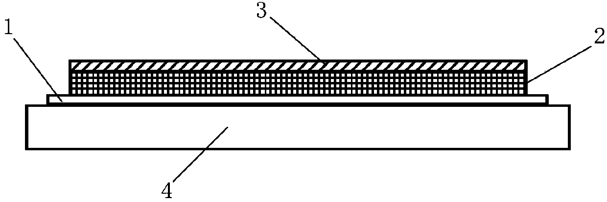
[0039] refer to figure 1 As shown, the secondary electron emission film has a multi-layer structure, including a buffer layer 1 , a mixed layer of magnesium oxide and metal 2 and a layer of magnesium oxide 3 arranged on a metal substrate 4 in sequence.

[0040] A kind of preparation method of secondary electron emission thin film of the present invention, comprises the following steps:

[0041] Firstly, a buffer layer 1 is deposited on the metal substrate 4 by sputtering a target made of one material among titanium, nickel, chromium, gold, silver, platinum or a composite target made of several of them, with a thickness of 3-100nm ;

[0042] Next, a magnesium oxide and metal mixed layer 2 is deposited on the buffer layer 1, which is a magnesium oxide cermet formed by simultaneously depositing magnesium oxide and metals by co-sputtering a magnesium target (or magnesium oxide target) and other metal targets layer, in which the other metal target is a target material of gold, si...

Embodiment 2

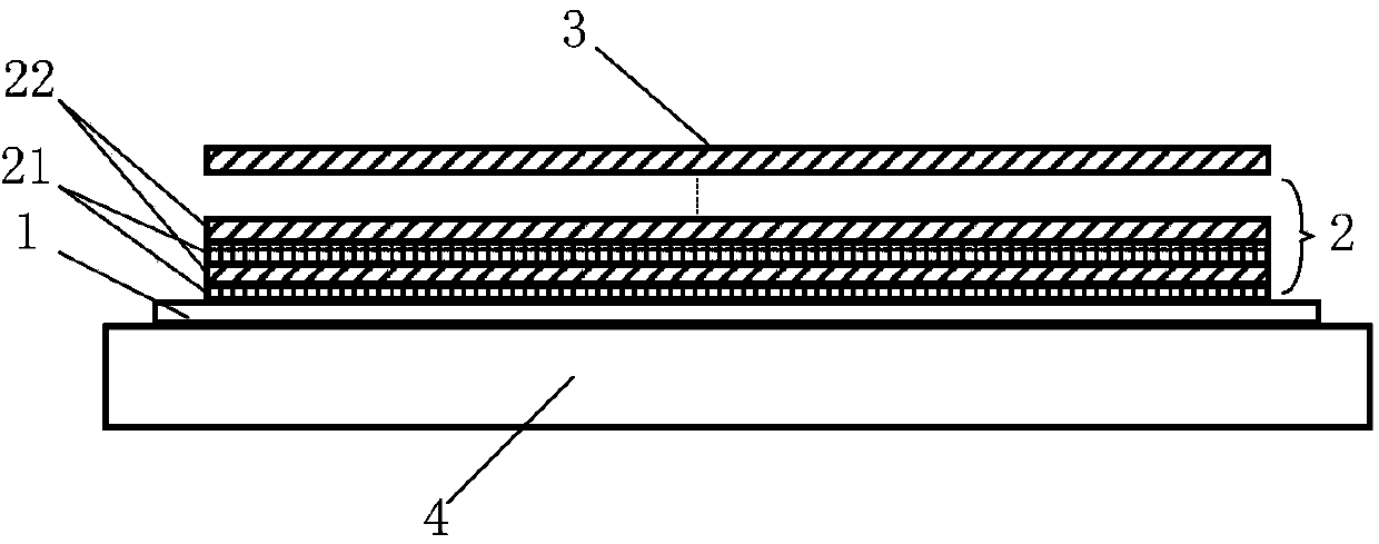
[0045] refer to figure 2 As shown, the secondary electron emission film has a multi-layer structure, including a buffer layer 1 , a mixed layer of magnesium oxide and metal 2 and a layer of magnesium oxide 3 arranged on a metal substrate 4 in sequence.

[0046] A kind of preparation method of secondary electron emission thin film of the present invention, comprises the following steps:

[0047] First, deposit a buffer layer 1 on the metal substrate 4 by sputtering a target made of one of titanium, nickel, chromium, gold, silver, and platinum, or a composite target consisting of several of these materials, with a thickness of 3-100nm between;

[0048] Next, the mixed layer 2 of magnesium oxide and metal is deposited on the buffer layer 1. The mixed layer 2 of magnesium oxide and metal is deposited by continuous sputtering of magnesium target (or magnesium oxide target) and intermittent sputtering of other metal targets. Magnesium oxide cermet layer 21 and magnesium oxide lay...

Embodiment 3

[0051] refer to image 3 As shown, the secondary electron emission film has a multi-layer structure, including a buffer layer 1 , a mixed layer of magnesium oxide and metal 2 and a layer of magnesium oxide 3 arranged on a metal substrate 4 in sequence.

[0052] A kind of preparation method of secondary electron emission thin film of the present invention, comprises the following steps:

[0053] Firstly, a buffer layer 1 is deposited on the metal substrate 4 by sputtering a target made of one material among titanium, nickel, chromium, gold, silver, platinum or a composite target made of several of them, with a thickness of 3-100nm ;

[0054] Next, a mixed layer 2 of magnesium oxide and metal is deposited on the buffer layer 1. The mixed layer 2 of magnesium oxide and metal is deposited by alternately sputtering a magnesium target (or magnesium oxide target) and other metal targets to deposit multiple alternating metal layers 23 and Magnesium oxide layer 24, wherein other meta...


PUM

PropertyMeasurementUnit
thicknessaaaaaaaaaa
thicknessaaaaaaaaaa
thicknessaaaaaaaaaa

Abstract

The invention discloses a preparation method of a secondary-electron emission thin film. The preparation method comprises the following steps: (1) depositing a buffer layer on a metal substrate; (2) depositing a magnesium oxide and metal mixed layer on the buffer layer by sputtering a magnesium target/magnesium oxide target and sputtering other metal targets; (3) depositing a surface on the magnesium oxide and metal mixed layer. In the step (2), the two targets are used for respectively depositing magnesium oxide and other metals, the sputtering power, the sputtering time, the flow rates of working gas and reactant gas and the temperature of the substrate are individually controlled so as to prepare the magnesium oxide and metal mixed layer with proper magnesium oxide and metal grain size, magnesium oxide crystallization orientation, metal content and distribution of metal grains in a membrane layer and thickness of the membrane layer. The secondary-electron emission thin film prepared by the method has high secondary electron emission yield and good electrical conductivity, and therefore, the secondary-electron emission thin film has high secondary-electron emission stability.

Description

technical field [0001] The invention belongs to the technical field of optoelectronic materials and devices, and relates to a preparation method of a secondary electron emission film that can be used for an electron multiplier. Background technique [0002] Magnesium oxide (MgO) thin films are widely used in image intensifiers, photomultiplier tubes, electron multipliers, orthogonal field amplifiers and devices such as plasma displays. When used in an electron multiplier, in order to obtain a long service life of the device, the secondary electron emission film must be able to withstand the long-term bombardment of a high-power electron current, so the thickness of the prepared MgO film needs to reach tens of nanometers or even a hundred above nanometers. However, since magnesium oxide is an insulating material, the thicker MgO film will produce surface charging phenomenon under the bombardment of electron flow, which will make its secondary electron emission coefficient d...

Claims


Application Information

Patent Timeline
Patent Type & Authority Applications(China)
IPC IPC(8): C23C14/16C23C14/06C23C14/08C23C14/34
Inventor 胡文波吴胜利徐琳魏强李亨付马龙
Owner XI AN JIAOTONG UNIV
Why Eureka
Try Eureka