Interface structure of micro-fluidic chip, and manufacturing method and application thereof

A microfluidic chip and interface structure technology, applied in chemical instruments and methods, laboratory containers, laboratory utensils, etc. Improve overall strength, improve tightness, and ensure the effect of strength and sealing

Inactive Publication Date: 2014-05-28
THE NAT CENT FOR NANOSCI & TECH NCNST OF CHINA
View PDF3 Cites 13 Cited by
  • Summary
  • Abstract
  • Description
  • Claims
  • Application Information

AI Technical Summary

Problems solved by technology

[0005] At present, people at home and abroad have paid attention to this problem and proposed some solutions, such as O-ring sealing method, direct intubation method and sealing method with epoxy glue, etc., but these methods still have complex production methods and sealing problems. Problems such as instability and low pressure resistance

Method used


Image

  • Interface structure of micro-fluidic chip, and manufacturing method and application thereof
  • Interface structure of micro-fluidic chip, and manufacturing method and application thereof
  • Interface structure of micro-fluidic chip, and manufacturing method and application thereof

Examples


Embodiment 1

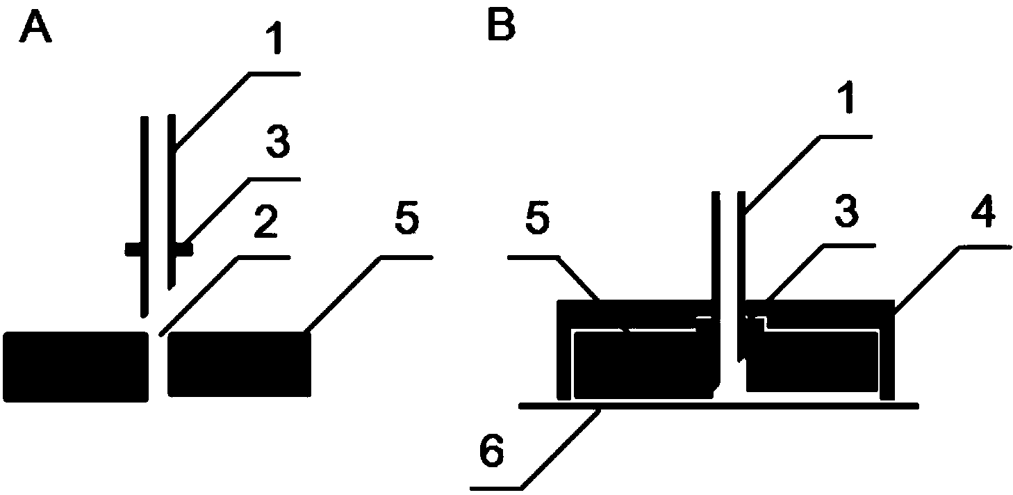
[0041] In this example, the uncured PDMS is prepared into a mixed solution according to the ratio of monomer and curing agent 10:1 (v:v), poured into the mold, and cured at 80°C for 2 hours (or cured at 100°C 15min), forming a microfluidic chip with a thickness of about 4-6mm, one of which has a channel surface.

[0042] Take out the microfluidic chip from the mold, use a puncher with an inner diameter of 0.5 mm and an outer diameter of 0.81 mm to punch a circular through hole connecting the outside world and the channel on the back of the channel surface, as the microfluidic channel inlet / outlet, and use For sample inflow or product or reaction waste outflow.

[0043] After drilling, take a PE drainage tube with an outer diameter of 1 mm, apply a small amount of uncured Dow Coning 3145 series silica gel on its port, and then insert the drainage tube into the microfluidic channel inlet / outlet pre-punched on the microfluidic chip The two form an interference fit, and the drain...

Embodiment 2

[0047] In this example, PMMA is melted at 240-270°C, poured into a mold with a temperature of 35-70°C, and after it is solidified, a microfluidic chip with a thickness of about 4-6mm is formed, one side of which has a channel noodle.

[0048] Take out the microfluidic chip from the mold, use a puncher with an inner diameter of 0.5 mm and an outer diameter of 0.81 mm to punch a circular through hole connecting the outside world and the channel on the back of the channel surface, as the microfluidic channel inlet / outlet, and use For sample inflow or product or reaction waste outflow.

[0049] After drilling, take a PEEK drainage tube with an outer diameter of 1 mm, apply a small amount of uncured Dow Coning 3145 series silica gel on its port, and then insert the drainage tube into the microfluidic channel inlet / outlet pre-punched on the microfluidic chip The two form an interference fit, and the drainage tube is firmly fixed in the inlet / outlet of the microfluidic channel.

[...

Embodiment 3

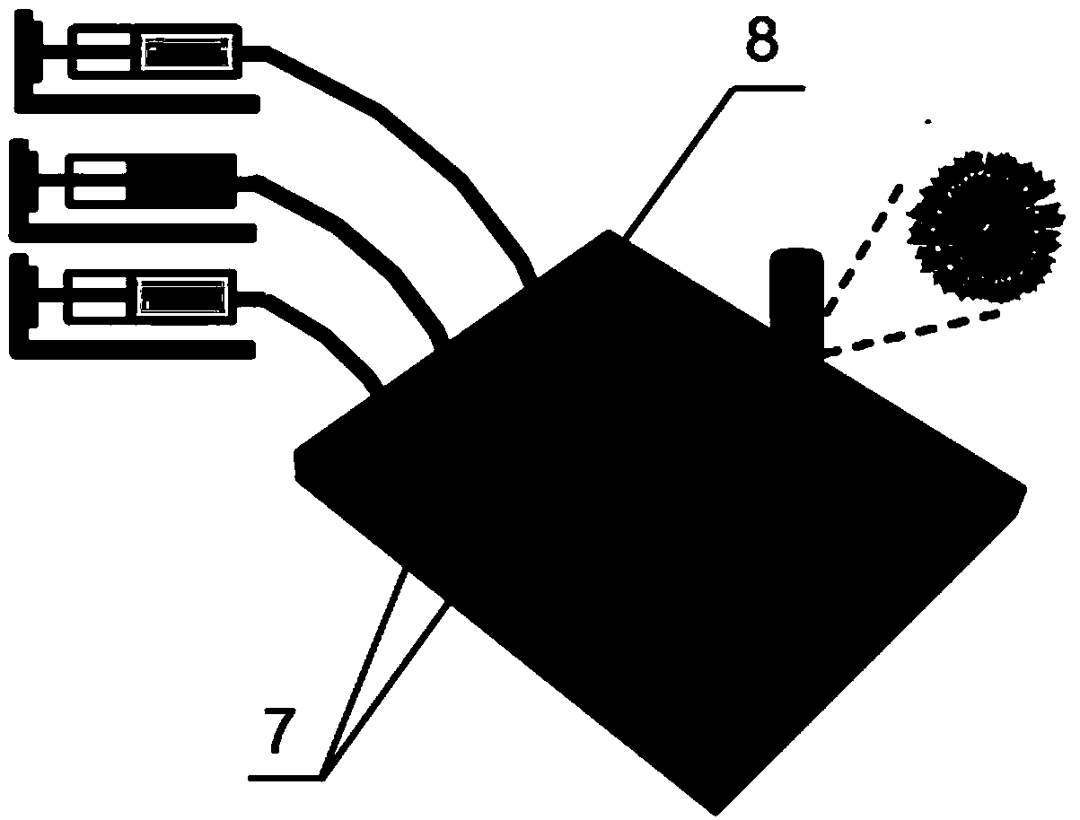
[0053] In this example, the interface structure of the microfluidic chip produced in Example 1 is used in the high-throughput synthesis of nanoparticles. Please refer to figure 2 , the interface structure of the water phase inlet 7 and the organic phase inlet 8 of the microfluidic device of this embodiment is made according to the method described in Example 1, and the sealing of the microfluidic device is completed. Pass into pure water from water phase inlet 7, pass into 2wt% PLGA solution (ie polylactic acid-glycolic acid copolymer solution, solvent is N,N-dimethylformamide) from organic phase inlet 8, water phase and organic phase The flow rate ratio of the three inlets can be adjusted as needed, and the flow rate ratio of the three inlets is preferably 200 (water phase): 10 (organic phase): 200 (water phase). Due to the extremely high flow rate ratio, the liquid is strongly mixed at the inlet, so that PLGA is rapidly precipitated from the solution, so that PLGA nanopart...


PUM


Abstract

The invention relates to an interface structure of a micro-fluidic chip, and a manufacturing method and an application thereof. The interface structure of the micro-fluidic chip comprises a drainage tube, a micro-fluidic channel inlet / outlet, a first seal layer and a second seal layer, wherein the drainage tube is inserted into the micro-fluidic channel inlet / outlet to form an interference fit; the first seal layer is sealant; the sealant bonds the drainage tube and the micro-fluidic channel inlet / outlet; the material of the second seal layer is the same as that of the micro-fluidic chip; the second seal layer covers the first seal layer and is adhered with the micro-fluidic chip and the drainage tube. The interface structure provided by the invention has the characteristics of firm seal and high pressure resistance, and can meet experiment requirements of high throughput synthesis of the micro-fluidic chip with relatively high flow speed.

Description

technical field [0001] The invention relates to the technical field of sealing of microfluidic channels, in particular to an interface structure of a microfluidic chip, a manufacturing method thereof, and an application in sealing of a microfluidic device. Background technique [0002] Microfluidic technology is a technology developed in recent years to control fluid flow at the micro / nano scale. Because of its convenient use and low price, it has been widely used in the fields of biological analysis, cell and microbial culture, and drug synthesis and screening. It is the basis for the next generation of pathogen detection, biological research, and drug synthesis and screening platforms. [0003] Polydimethylsiloxane (PDMS) is a polymer with outstanding advantages such as good light transmission and high biocompatibility. Microfluidic chips with PDMS as the main material have been widely used in pathogen detection, cell And microbial culture and drug synthesis screening and...

Claims


Application Information

Patent Timeline
Patent Type & Authority Applications(China)
IPC IPC(8): B01L3/00
Inventor 蒋兴宇王纪东孙佳姝靳钰
Owner THE NAT CENT FOR NANOSCI & TECH NCNST OF CHINA
Why Eureka
Try Eureka