Preparation method for shape-controllable silver nanosheet assembly structure array and application of shape-controllable silver nanosheet assembly structure array
A technology of silver nanosheets and assembled structures, which is applied in nanotechnology, nanotechnology, nanotechnology, etc. for materials and surface science, and can solve problems such as restricting use occasions and application fields, increasing complexity and cost, and single product , to achieve the effects of expanding use occasions and application fields, enriching optical properties, and scientific preparation methods
- Summary
- Abstract
- Description
- Claims
- Application Information
AI Technical Summary
Problems solved by technology
Method used
Image
Examples
Embodiment 1
[0028] The specific steps of preparation are:
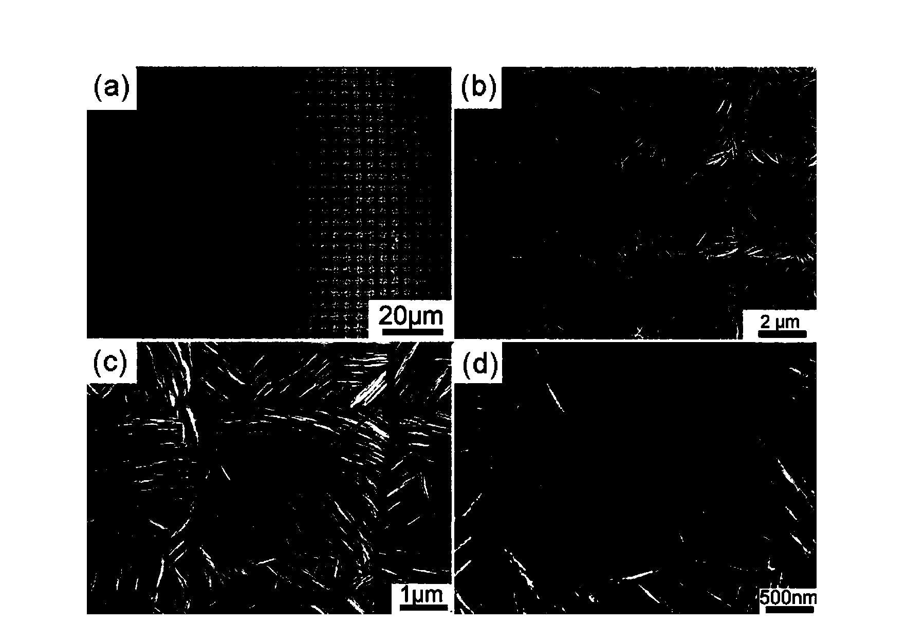
[0029] Step 1, first place the inert conductive substrate in a vacuum evaporation apparatus, at a current density of 8mA / cm 2 The gold is evaporated for 24 s to obtain an inert conductive substrate covered with a gold film; wherein, the inert conductive substrate is a conductive glass substrate. Then, a positive photoresist with a thickness of 1 μm was coated on the inert conductive substrate covered with gold film, and it was dried at 90 °C for 20 min to obtain an inert conductive substrate covered with positive photoresist and gold film in turn. ; Among them, the coating is spin coating, the rotation speed during spin coating is 4000r / min, and the time is 20s.
[0030] Step 2, cover the photolithography plate with an ordered array of light-transmitting patterns on the inert conductive substrate sequentially covered with positive photoresist and gold film, and then expose it to ultraviolet light for 36 s; The light transmissio...
Embodiment 2
[0033] The specific steps of preparation are:
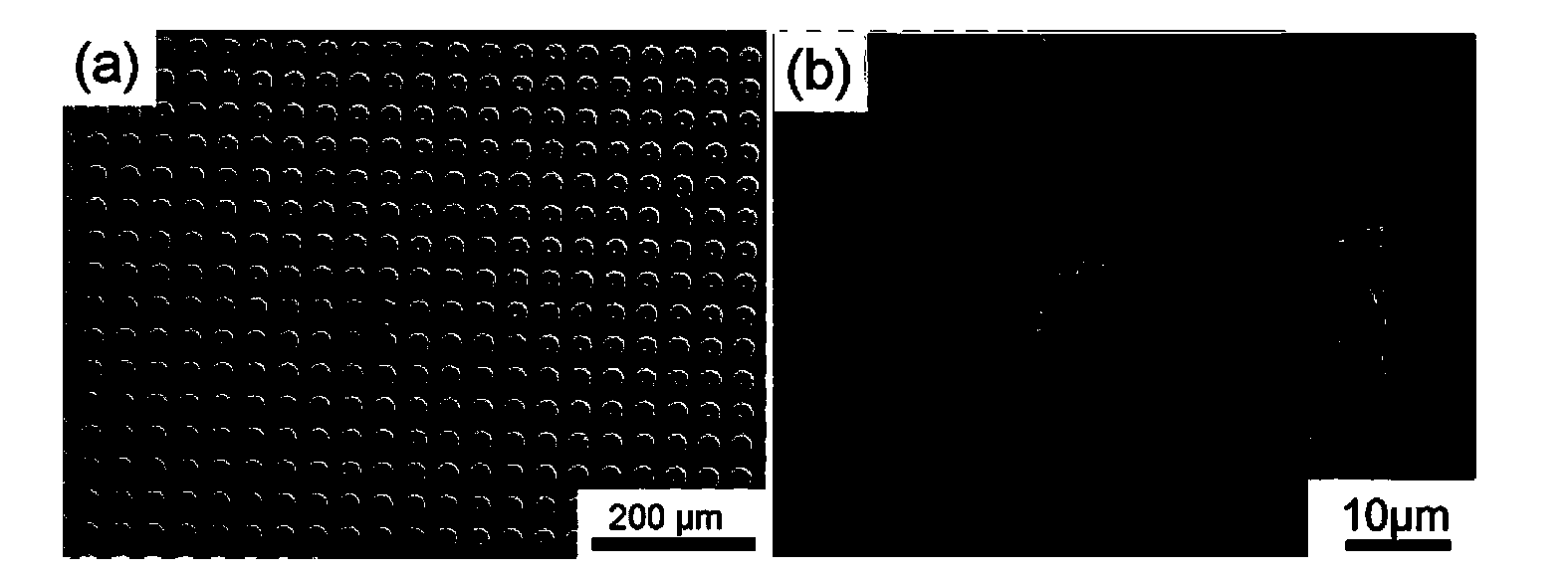
[0034] Step 1, first place the inert conductive substrate in a vacuum evaporation apparatus, at a current density of 9mA / cm 2 The gold is evaporated for 23 s to obtain an inert conductive substrate covered with a gold film; wherein, the inert conductive substrate is a conductive glass substrate. Then, a positive photoresist with a thickness of 1.1 μm was coated on the inert conductive substrate covered with the gold film, and it was dried at 93 °C for 19 min to obtain an inert conductive substrate covered with positive photoresist and gold film in sequence. The substrate; wherein, the coating is spin coating, the rotational speed during spin coating is 4000r / min, and the time is 20s.
[0035] Step 2, firstly cover the photolithography plate with an ordered array of light-transmitting patterns on the inert conductive substrate covered with positive photoresist and gold film in sequence, and then expose it to ultraviolet light for...
Embodiment 3
[0038] The specific steps of preparation are:
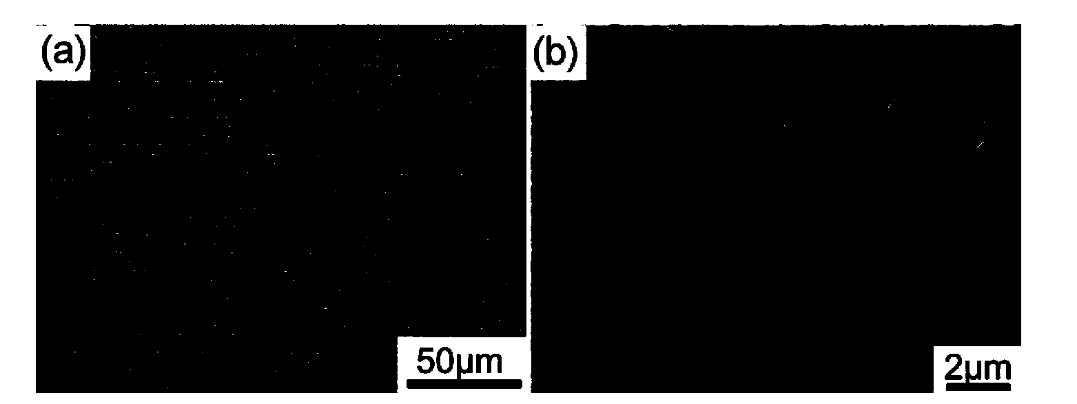
[0039] Step 1, first place the inert conductive substrate in a vacuum evaporation apparatus, at a current density of 10mA / cm 2 The gold is evaporated for 22 s to obtain an inert conductive substrate covered with a gold film; wherein, the inert conductive substrate is a conductive glass substrate. Then, a positive photoresist with a thickness of 1.2 μm was coated on the inert conductive substrate covered with gold film, and it was dried at 95 °C for 17 min to obtain an inert conductive substrate covered with positive photoresist and gold film in sequence. The substrate; wherein, the coating is spin coating, the rotational speed during spin coating is 4000r / min, and the time is 20s.
[0040] Step 2, firstly cover the photolithography plate with an ordered array of light-transmitting patterns on the inert conductive substrate covered with positive photoresist and gold film in sequence, and then expose it to ultraviolet light for 38...
PUM
 Abstract
Description
Claims
Application Information


