Copper alloy for electronic equipment, method for producing copper alloy for electronic equipment, rolled copper alloy material for electronic equipment, and part for electronic equipment

A technology for electronic equipment and manufacturing methods, which is applied in cable/conductor manufacturing, conductive materials, conductive materials, etc., can solve the problems of components for electronic equipment that cannot be formed into shapes, high tensile elastic modulus, plastic deformation, etc., and achieves excellent resistance. Effects of stress relaxation properties, low tensile elastic modulus, and high electrical conductivity

Active Publication Date: 2014-06-04
MITSUBISHI MATERIALS CORP
View PDF6 Cites 6 Cited by
  • Summary
  • Abstract
  • Description
  • Claims
  • Application Information

AI Technical Summary

Problems solved by technology

Among them, in a connector with a structure in which the tab pushes up the spring contact part of the female terminal and is inserted, if the tensile modulus of the material constituting the connector is high, there may be a sharp change in the contact pressure during insertion. , and it is easy to deform plastically beyond the elastic limit, so it is not preferred
[0014] In addition, in the Cu-Mg alloys described in Non-Patent Document 2 and Patent Document 3, intermetallic compounds are precipitated in the same way as Corson copper-nickel-silicon alloys, so there is a tendency for the tensile modulus to be high. Connectors are not preferred
[0015] In addition, in the Cu-Mg alloy, many coarse intermetallic compounds are dispersed in the parent phase, so these intermetallic compounds are likely to become starting points during bending, causing cracks, etc., so there is a problem that components for electronic devices with complex shapes cannot be molded. question

Method used


Image

  • Copper alloy for electronic equipment, method for producing copper alloy for electronic equipment, rolled copper alloy material for electronic equipment, and part for electronic equipment
  • Copper alloy for electronic equipment, method for producing copper alloy for electronic equipment, rolled copper alloy material for electronic equipment, and part for electronic equipment
  • Copper alloy for electronic equipment, method for producing copper alloy for electronic equipment, rolled copper alloy material for electronic equipment, and part for electronic equipment

Examples


Embodiment

[0125] Hereinafter, the results of confirmation experiments conducted to confirm the effects of the present invention will be described.

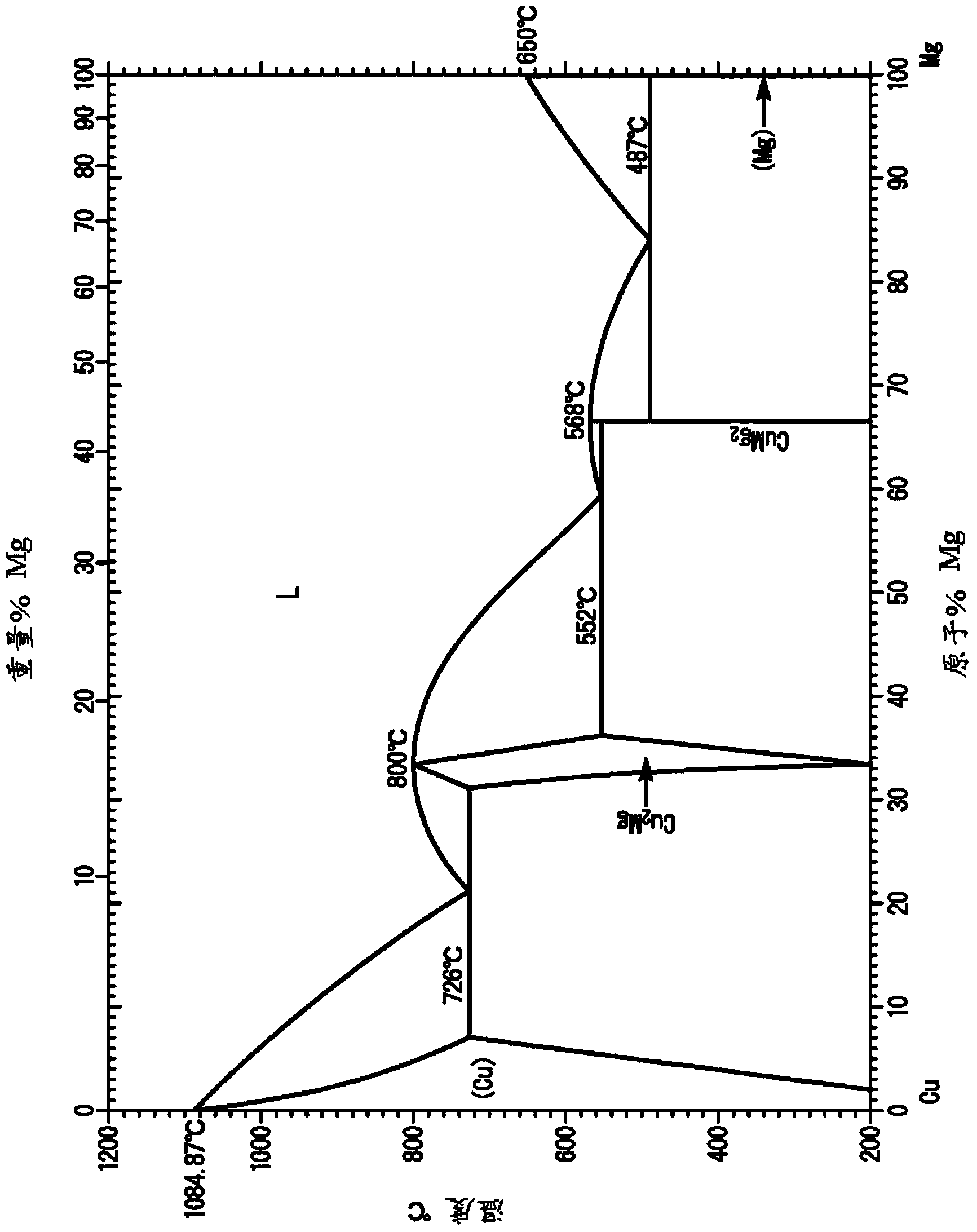
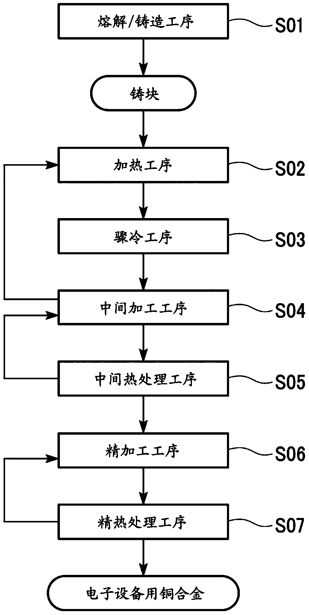
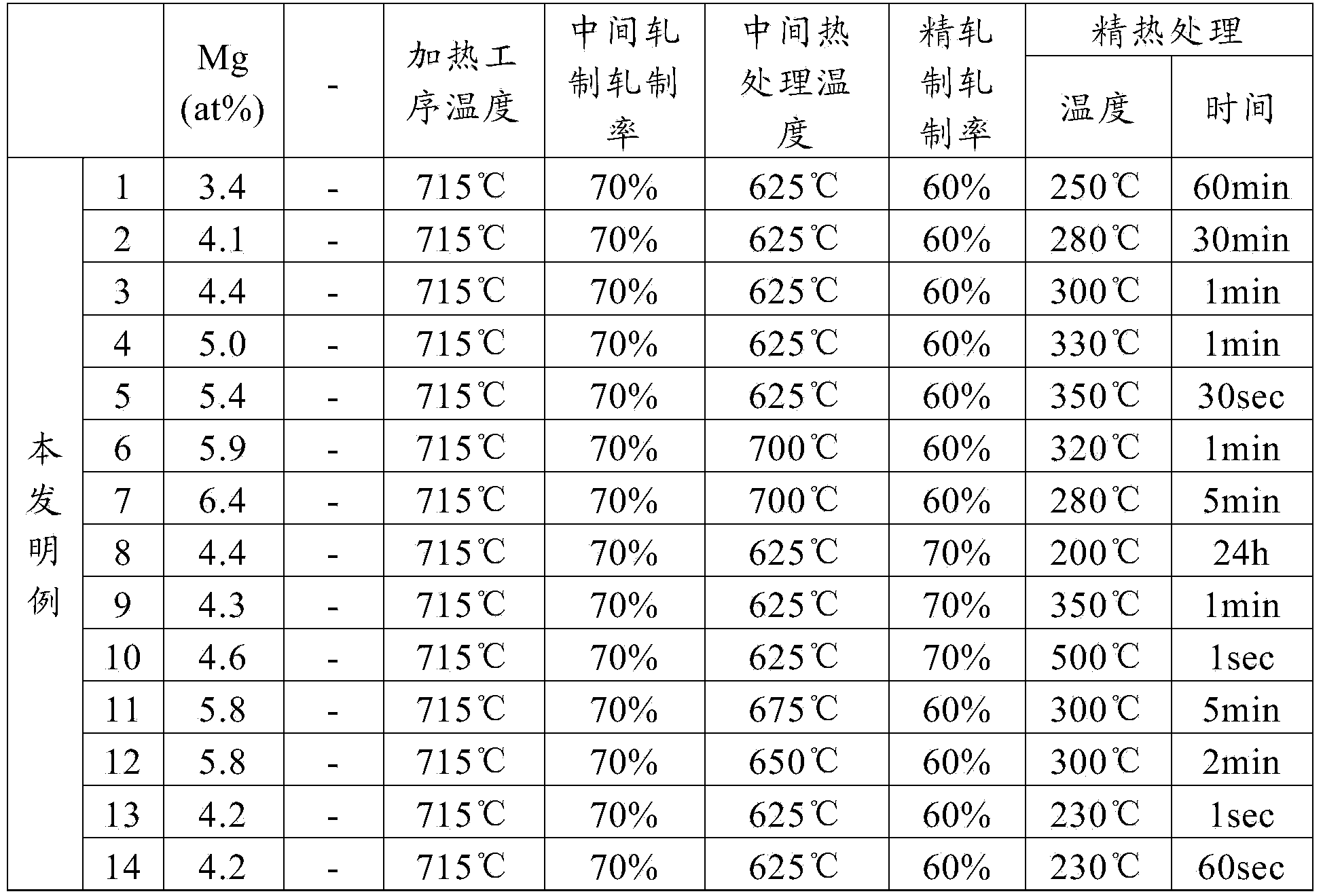
[0126] A copper raw material composed of oxygen-free copper (ASTM B152C10100) with a purity of 99.99% by mass or higher was prepared, and the copper raw material was placed in a high-purity graphite crucible and subjected to high-frequency melting in an atmosphere furnace set to an Ar gas atmosphere. Various additive elements were added to the obtained molten copper to prepare the component compositions shown in Tables 1 and 2, and cast into carbon molds to produce ingots. In addition, the size of the ingot was about 20 mm in thickness×about 20 mm in width×about 100 to 120 mm in length.

[0127] The obtained ingot was heated in an Ar gas atmosphere for 4 hours under the temperature conditions described in Tables 1 and 2, and then water quenched (cooling temperature 20° C., cooling rate 1500° C. / min).

[0128] The heat-treated ingot is cut,...


PUM

PropertyMeasurementUnit
yield strengthaaaaaaaaaa
particle diameteraaaaaaaaaa
crystal sizeaaaaaaaaaa

Abstract

A copper alloy for electronic equipment comprises between 3.3 at% and 6.9 at% of Mg, with the balance being substantially Cu and inevitable impurities. When the Mg concentration is X at%, the conductivity sigma (% IACS) is within a range of sigma < {1.7241/(-0.0347 X2 + 0.6569 X + 1.7)} 100, and the stress relaxation percentage after 1,000 hours at 150 C is 50% or less.

Description

technical field [0001] The present invention relates to a copper alloy for electronic equipment suitable for components for electronic equipment such as terminals, connectors, relays, and lead frames, a method for manufacturing a copper alloy for electronic equipment, a rolled copper alloy material for electronic equipment, and components for electronic equipment . [0002] This application claims priority based on Japanese Patent Application No. 2011-237800 for which it applied in Japan on October 28, 2011, and uses the content for this specification. Background technique [0003] Conventionally, along with miniaturization of electronic equipment and electric equipment, components for electronic equipment such as terminals, connectors, relays, and lead frames used in these electronic equipment and electric equipment have been required to be miniaturized and thinned. Therefore, copper alloys excellent in elasticity, strength, and electrical conductivity are required as mate...

Claims


Application Information

Patent Timeline
Patent Type & Authority Applications(China)
IPC IPC(8): C22F1/08C22C9/00H01B5/02H01B13/00C22F1/00
CPCH01B13/00H01B1/026C22C9/05C22C9/02C22F1/08C22F1/00H01B5/02C22C9/00H01B13/0016
Inventor 牧一诚伊藤优树
Owner MITSUBISHI MATERIALS CORP
Why Eureka
Try Eureka