Photoresist remover

A photoresist and remover technology, applied in optics, optomechanical equipment, detergent compositions, etc., can solve the problems of strong corrosiveness and insufficient cleaning ability of semiconductor wafer patterns and substrates

Inactive Publication Date: 2014-06-18
ANJI MICROELECTRONICS TECH (SHANGHAI) CO LTD
View PDF7 Cites 16 Cited by
  • Summary
  • Abstract
  • Description
  • Claims
  • Application Information

AI Technical Summary

Problems solved by technology

[0005] The technical problem to be solved by the present invention is to provide a method for cleaning thick-film photoresist in view of the insufficient cleaning ability of existing thick-film photoresist cleaning solutions or the defects of strong corrosion to semiconductor wafer patterns and substrates. Highly capable photoresist cleaner with low corrosiveness to semiconductor wafer patterns and substrates

Method used


Image

  • Photoresist remover
  • Photoresist remover
  • Photoresist remover

Examples


Embodiment Construction

[0019] The reagents and raw materials used in the present invention are all commercially available. The cleaning solution of the present invention can be prepared by simply and uniformly mixing the above components.

[0020] The advantages of the present invention will be further elaborated below through specific embodiments. But the present invention includes, but is not limited to, the specific compositions of the following examples.

[0021] Preparation Example

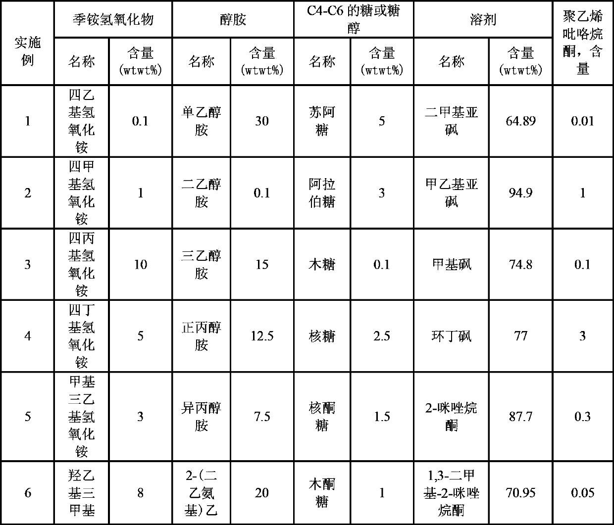
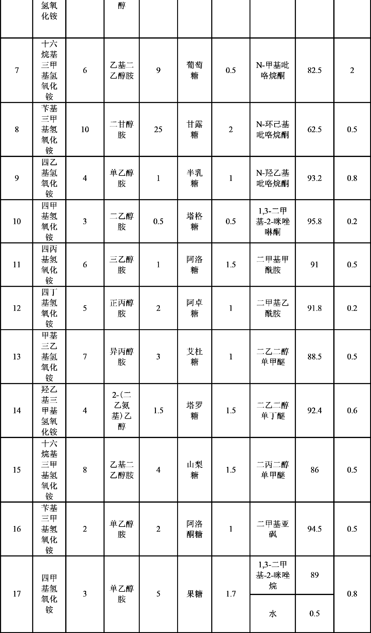
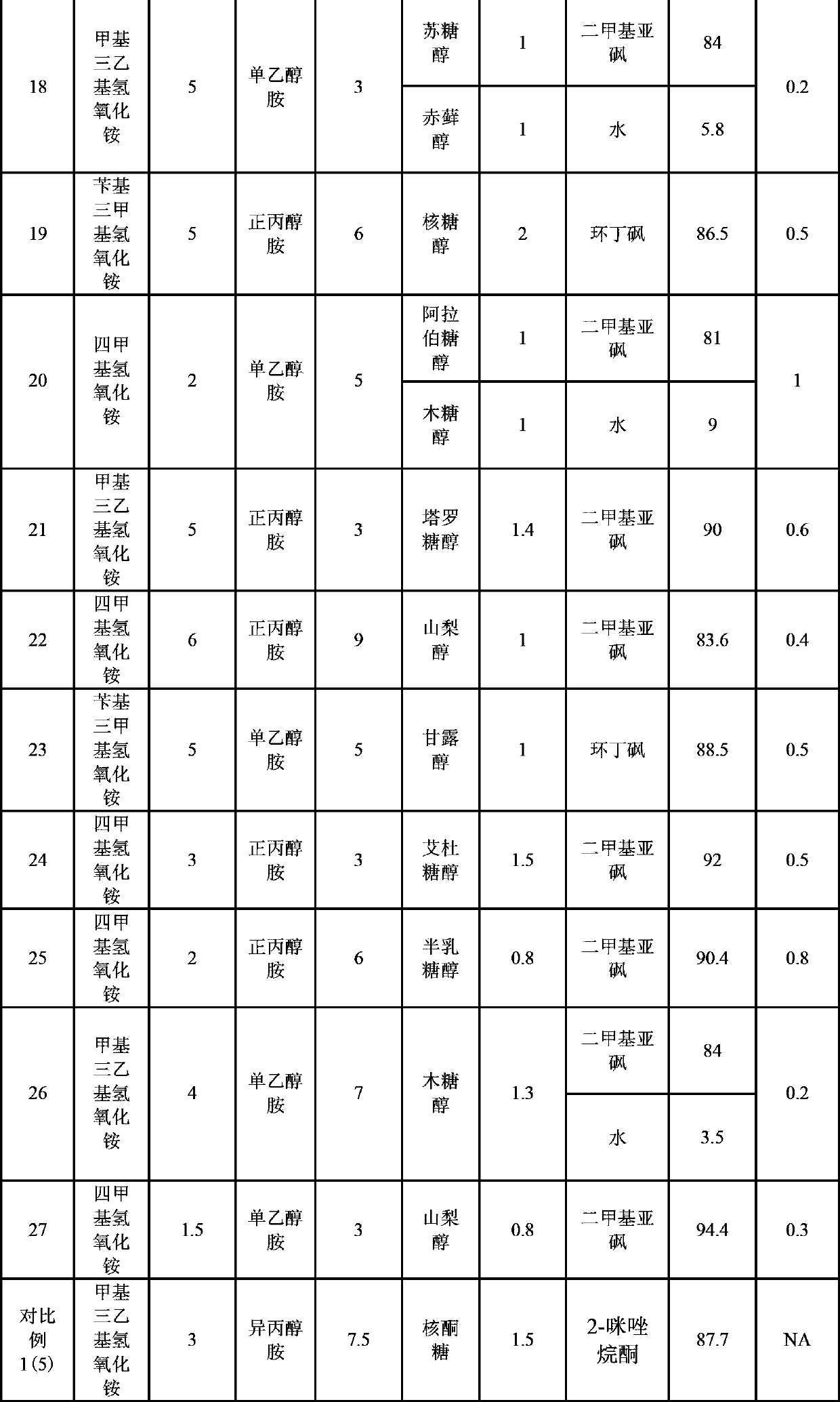
[0022] Table 1 provides the cleaning solution formula of the present invention. The percentages described below are all mass percentages.

[0023] Table 1 Components and contents of cleaning agents in Examples and Comparative Examples

[0024]

[0025]

[0026]

[0027]

[0028] In order to further investigate the cleaning situation of this type of cleaning solution, the present invention adopts the following technical means: immerse the wafer containing photoresist in the cleaning agent, and use a ...


PUM


Abstract

The invention discloses a low etching resist cleaning fluid suitable for cleaning of thicker photoresists. The low etching resist photoresist cleaning fluid comprises (a) a quaternary ammonium hydroxide, (b) an alkylol amine, (c) a sugar or a sugar alcohol, (d) a surfactant, and (e) a solvent. The low etching resist photoresist cleaning fluid is capable of removing the photoresists on semiconductor wafers with high efficiency; no attack on base materials, such as aluminium and copper, is caused; and the low etching resist photoresist cleaning fluid processing a promising application prospect in the field of semiconductor wafer cleaning.

Description

technical field [0001] The invention relates to a photoresist remover. Background technique [0002] In the usual semiconductor manufacturing process, a photoresist mask is formed on the surface of some materials, and the pattern is transferred after exposure. After the required pattern is obtained, the remaining photoresist needs to be peeled off before the next process. . This process requires complete removal of unwanted photoresist without etching any substrate. For example, in the wafer microsphere implantation process (bumping technology), a photoresist is required to form a mask, and the mask also needs to be removed after the microspheres are successfully implanted, but because the photoresist is relatively thick, it is often difficult to completely remove more difficult. The more common methods to improve the removal effect are to extend the soaking time, increase the soaking temperature and use more aggressive solutions, but this often causes corrosion of the wa...

Claims


Application Information

Patent Timeline
Patent Type & Authority Applications(China)
IPC IPC(8): G03F7/42
CPCC11D7/34C11D3/43C11D11/0047C11D7/32G03F7/42C11D3/22C11D3/30C11D7/26G03F7/425
Inventor 刘兵彭洪修孙广胜颜金荔
Owner ANJI MICROELECTRONICS TECH (SHANGHAI) CO LTD
Why Eureka
Try Eureka