
High-resistance and low-dislocation GaN thin film and preparation method

A low-dislocation, high-resistance technology, applied in chemical instruments and methods, circuits, electrical components, etc., can solve problems such as reducing the quality of epitaxial film crystals

Inactive Publication Date: 2014-06-25
INST OF SEMICONDUCTORS - CHINESE ACAD OF SCI
View PDF3 Cites 7 Cited by
  • Summary
  • Abstract
  • Description
  • Claims
  • Application Information

AI Technical Summary

Problems solved by technology

This method is simple in process, but it will introduce high-density dislocations, which will greatly reduce the crystal quality of the epitaxial film

Method used


Image

  • High-resistance and low-dislocation GaN thin film and preparation method
  • High-resistance and low-dislocation GaN thin film and preparation method

Examples


Embodiment Construction

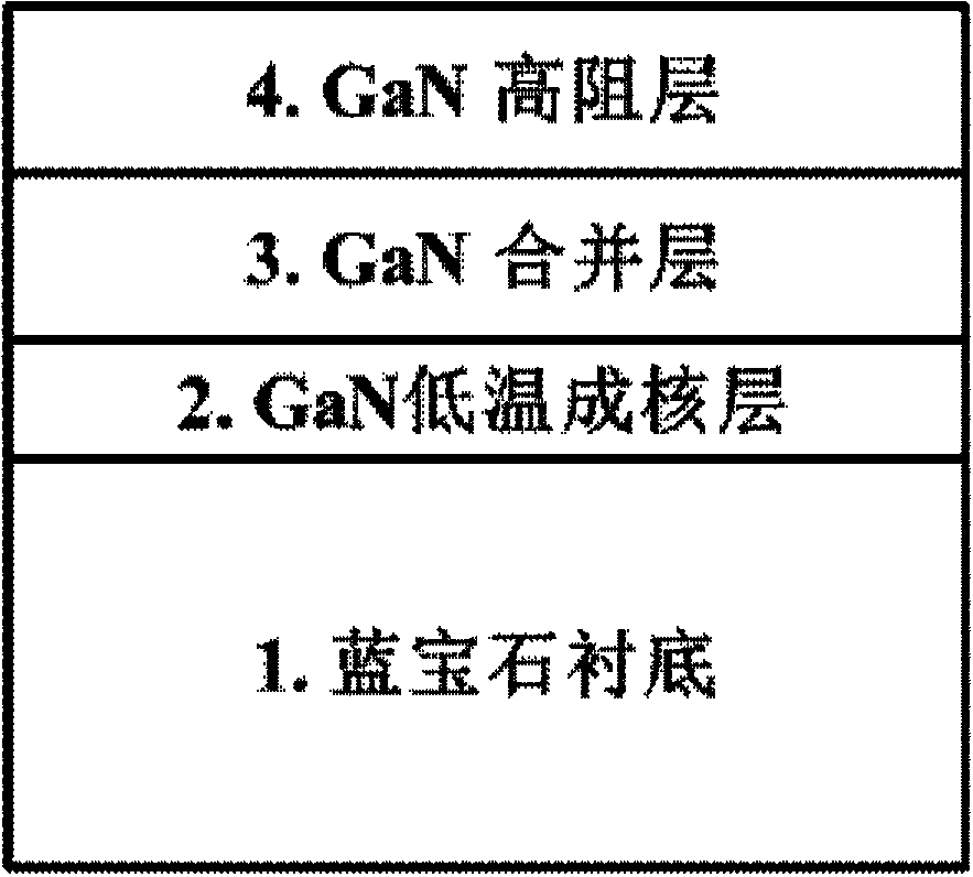
[0019] See figure 1 As shown, the present invention provides a high resistance low dislocation GaN film, including:

[0020] A substrate 1, the material of which is sapphire;

[0021] A GaN low-temperature nucleation layer 2 fabricated on the substrate 1. The growth temperature of the GaN low-temperature nucleation layer 2 is 500°C and 600°C, the pressure of the reaction chamber is 450550 Torr, and the thickness is 1525 nm;

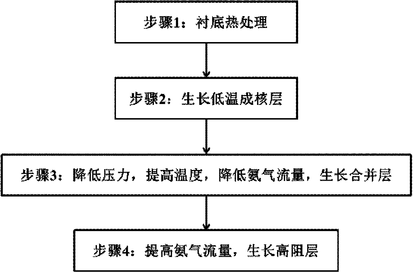
[0022] A GaN combined layer 3, which is fabricated on the GaN low-temperature nucleation layer 2. The growth temperature of the GaN combined layer 3 is 1000-1100°C, the reaction chamber pressure is 40-100 Torr, the ammonia flow rate is 0.2-1 SLM, and the thickness is 700-800nm;

[0023] The purpose of merging layer 3 is to reduce the dislocation density of the material and improve the quality of the material. The purpose of reducing the ammonia flow rate in the merged layer 3 is to make the material grow faster in the longitudinal direction than in the transvers...


PUM

PropertyMeasurementUnit
temperatureaaaaaaaaaa
thicknessaaaaaaaaaa
thicknessaaaaaaaaaa

Abstract

A high-resistance and low-dislocation GaN thin film comprises a substrate, a GaN low temperature nucleating layer which is made on the substrate, a GaN combined layer made on the GaN low temperature nucleating layer, and a GaN high-resistance layer made on the GaN combined layer. According to the high-resistance and low-dislocation GaN thin film, the intensity of pressure in a reaction chamber is controlled, and involuntary controllable carbon doping is realized, so that the purposes of compensating background charge carriers and improving the material electrical resistivity are achieved. The ammonia gas flow in the initial growth period is controlled, the combined layer is introduced, and the transition time from three-dimension growth to two-dimension growth of crystal is prolonged, so that the dislocation density of an epitaxial film is reduced under the premise that the high resistance rate of materials is ensured, and the purpose of improving crystal quality is achieved.

Description

Technical field [0001] The invention relates to the technical field of semiconductor materials, in particular to a GaN epitaxial film and a preparation method. Background technique [0002] In recent years, with the rise and rapid development of third-generation wireless communications and military phased array radars, high-power microwave devices such as high electron mobility transistors (HEMT) have received extensive attention and research. GaN has excellent characteristics such as large forbidden band width, high breakdown electric field, high electronic saturation drift speed, strong radiation resistance and good chemical stability; and it can form a heterojunction with AlGaN materials, and the pressure on the heterojunction interface Electric polarization and spontaneous polarization can generate high concentration of two-dimensional electron gas (2DEG), which is an excellent choice for manufacturing HEMT devices. [0003] However, GaN films grown by MOCVD technology are usu...

Claims


Application Information

Patent Timeline
Patent Type & Authority Applications(China)
IPC IPC(8): H01L29/06H01L29/778H01L21/205H01L21/335
CPCC30B25/14C30B25/20C30B29/406H01L21/0242H01L21/0254H01L21/0262
Inventor 何晓光赵德刚江德生刘宗顺陈平杨静乐伶聪李晓静杨辉
Owner INST OF SEMICONDUCTORS - CHINESE ACAD OF SCI
Learn More