Junction terminal applied to deep-groove super-junction device and manufacturing method thereof

A technology of superjunction devices and junction terminals, which is applied in semiconductor/solid-state device manufacturing, semiconductor devices, electrical components, etc., and can solve problems such as extremely high requirements for trench filling quality, increased etching and filling time, and increased process technical difficulty. , to achieve the effect of reducing etching and filling time, increasing capacity and good compatibility

Active Publication Date: 2014-06-25
QST CORP
View PDF5 Cites 9 Cited by
  • Summary
  • Abstract
  • Description
  • Claims
  • Application Information

AI Technical Summary

Problems solved by technology

The structure of P-pillars and N-pillars alternating with each other is adopted alone, the process technology difficulty is low, and the yield rate is high, but this junction terminal is a waste of area
The structure of filling the trench with high dielectric constant material alone can greatly reduce the area of ​​the junction terminal, but the width of the trench increases with the increase of the withstand voltage requirement of the device. With the increase of the trench width, the engraved The etching and filling time are also greatly increased, which reduces the production efficiency; at the same time, because the tr

Method used


Image

  • Junction terminal applied to deep-groove super-junction device and manufacturing method thereof
  • Junction terminal applied to deep-groove super-junction device and manufacturing method thereof
  • Junction terminal applied to deep-groove super-junction device and manufacturing method thereof

Examples


Embodiment 1

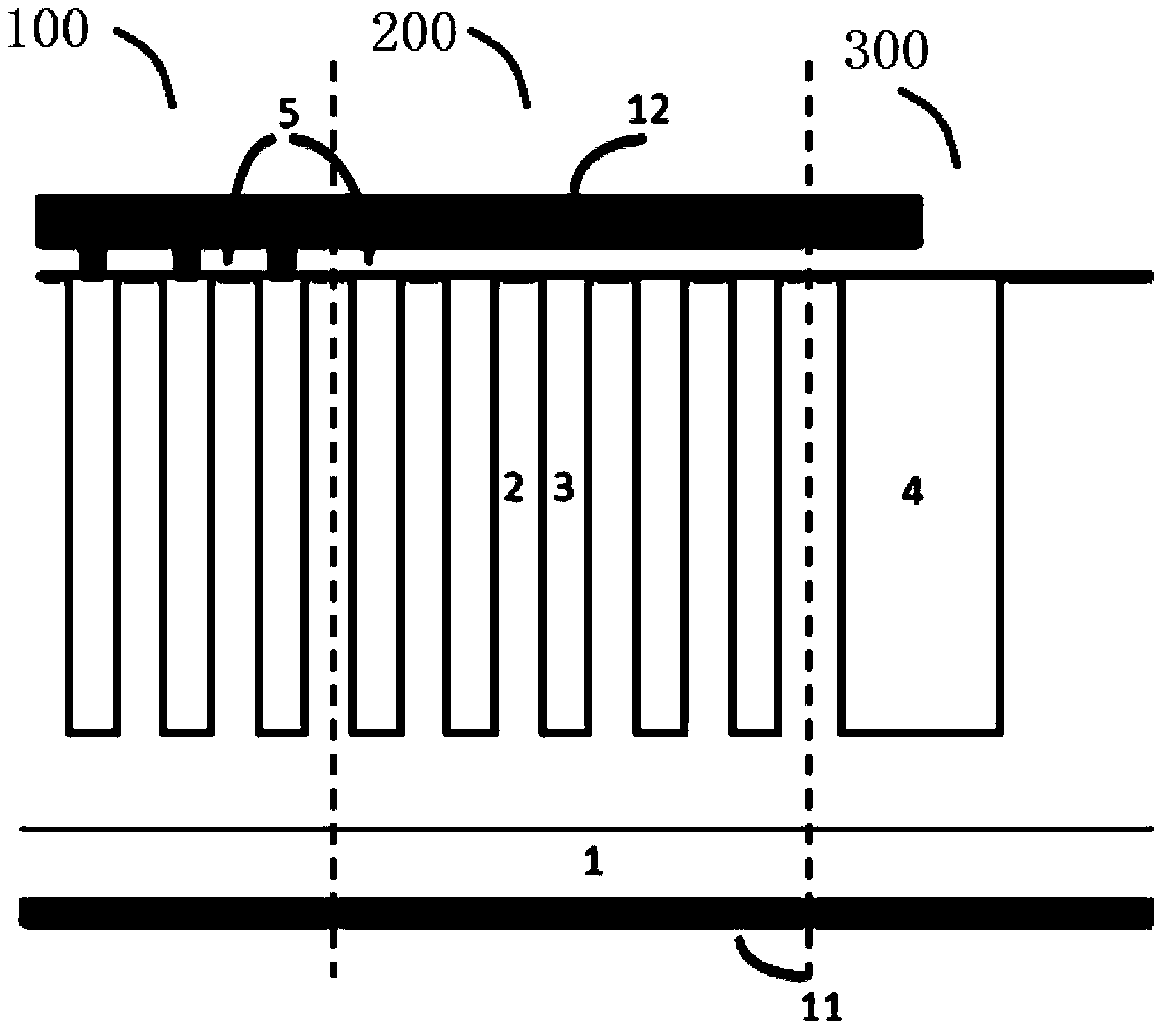
[0040] see figure 1 , the present invention discloses a junction terminal suitable for deep trench super junction devices, the junction terminal comprising: a semiconductor substrate 1, a first electrode 11, a semiconductor region 2, and a second electrode.

[0041] The semiconductor substrate 1 is a semiconductor material with a first doping type, with a doping resistivity of about 0.002-0.008 ohm.cm, typically an As or Sb doped N-type silicon substrate.

[0042] The first electrode 11 is formed on the lower end surface (back surface) of the semiconductor substrate 1; the semiconductor region 2 is formed on the upper end surface of the semiconductor substrate 1, which has the first conductivity type (ie, the first doping type), and the semiconductor region 2 A typical material is a Ph-doped N-type silicon epitaxial material with a resistivity of 1-10ohm.cm.

[0043] The semiconductor region includes: an active region, a first termination region, and a second termination regi...

Embodiment 2

[0053] The difference between this embodiment and Embodiment 1 is that in this embodiment, the preparation method of the junction terminal of the present invention includes the following steps:

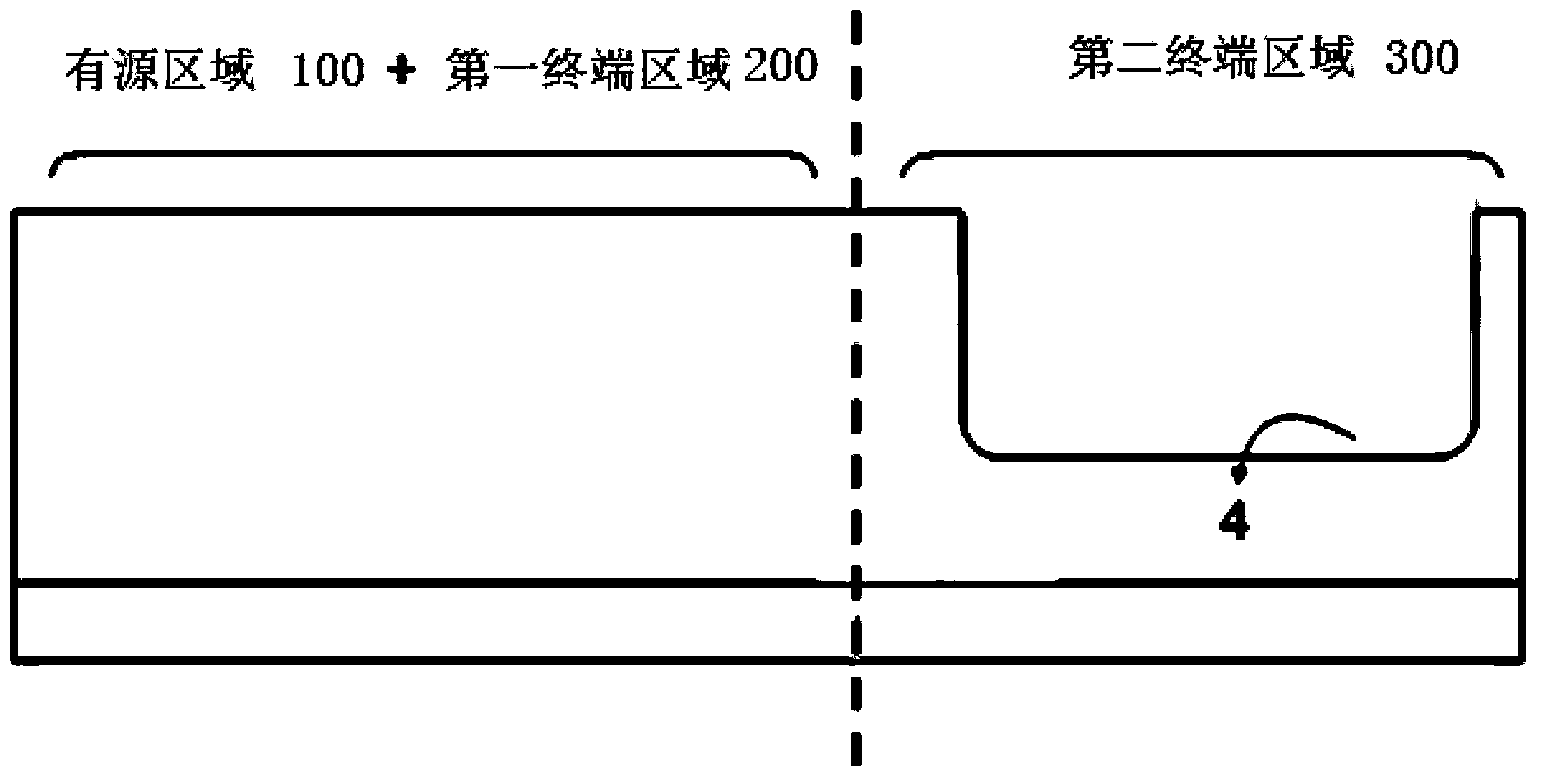
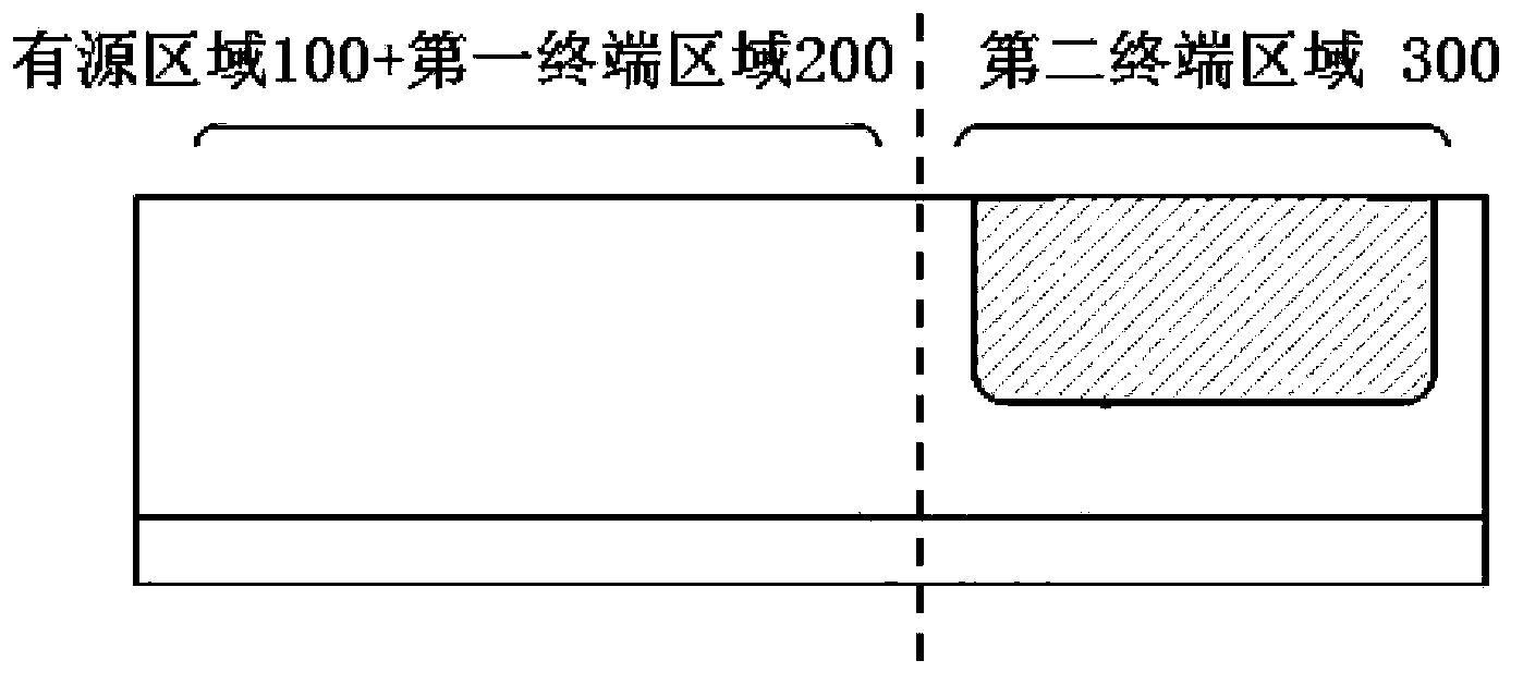
[0054] [Step S1] Combine figure 1 As shown, an N-type epitaxial layer (semiconductor region 2 ), such as a Ph-doped low-doped epitaxial layer with a thickness of 48 um, is grown on a heavily doped silicon substrate (semiconductor substrate 1 ). Then etch the fourth trench 6 of the terminal region 2 on the N-type epitaxial layer (such as Figure 4 ), the depth and width of the trench are determined by the withstand voltage of the device and the doping concentration of the substrate, and the trench opening size and its spacing are selected according to the reasonable design value of the oxidation process, and then completely oxidized by the method of growing silicon dioxide at high temperature silicon between the fourth trenches 6 in the terminal region two, and the oxide layer grown a...


PUM

PropertyMeasurementUnit
Thicknessaaaaaaaaaa

Abstract

The invention discloses a junction terminal applied to a deep-groove super-junction device and a manufacturing method thereof. The junction terminal comprises a semiconductor substrate, a first electrode, a semiconductor region, and a second electrode, wherein the first electrode is formed on the lower end surface of the semiconductor substrate; the semiconductor region is formed on the upper end surface of the semiconductor substrate and is provided with a first conductive type; the semiconductor region comprises an active region, a first terminal region, and a second terminal region. The active region is provided with a plurality of first grooves, and the first grooves are internally filled with semiconductor material with a second conductive type; the first terminal region is provided with a plurality of third grooves, and the third grooves are internally filled with semiconductor material with a second conductive type; the second terminal region is provided with a plurality of second grooves, and the second grooves are internally provided with insulated material with high dielectric constants. The second electrode is connected with the first grooves of the active region and covers the active region, the first terminal region and the second terminal region. The junction terminal of the invention can improve high voltage-resisting characteristics of the junction terminal device.

Description

technical field [0001] The invention belongs to the technical field of semiconductor power devices, relates to a junction terminal of a super junction device, in particular to a junction terminal suitable for a deep trench super junction device; at the same time, the invention also relates to a junction terminal suitable for a deep trench super junction device Preparation method of junction terminal. Background technique [0002] Modern power electronics technology has roughly the following requirements for the performance of power devices: 1) high withstand voltage, 2) high current density when turned on; 3) low voltage on the device when turned on, 4) high switching speed, 5) drive The power is small, the above points 3 and 4 are especially noteworthy. VDMOS, which appeared in 1980, has been used until now due to its high withstand voltage, fast switching speed, and low driving power. However, the traditional VDMOS on-resistance is limited by the "silicon limit" relation...

Claims


Application Information

Patent Timeline
IPC IPC(8): H01L29/78H01L29/06H01L21/336
CPCH01L29/0634H01L29/0649H01L29/66681H01L29/7816
Inventor 不公告发明人
Owner QST CORP
Why Eureka
Try Eureka