Manufacturing method for LED chip

A technology for light-emitting diodes and a manufacturing method, applied in semiconductor devices, electrical components, circuits, etc., can solve the problems of high cost, cumbersome process, unfavorable reflective layer formation, etc., so as to reduce manufacturing cost, increase reflective area, and reduce instability phenomenon Effect

Active Publication Date: 2014-07-02
ANHUI SANAN OPTOELECTRONICS CO LTD
View PDF14 Cites 11 Cited by
  • Summary
  • Abstract
  • Description
  • Claims
  • Application Information

AI Technical Summary

Problems solved by technology

However, this process is to dissociate into independent chips first and then do the coating process. The process is cumbersome and the cost is high; in addition, the side of the chip is a vertical surface, which is not conducive to the formation of the reflective layer (such as evaporation or sputtering, etc.)

Method used


Image

  • Manufacturing method for LED chip
  • Manufacturing method for LED chip
  • Manufacturing method for LED chip

Examples


Embodiment 1

[0034] A method for manufacturing a gallium nitride-based light-emitting diode chip, the manufacturing steps comprising:

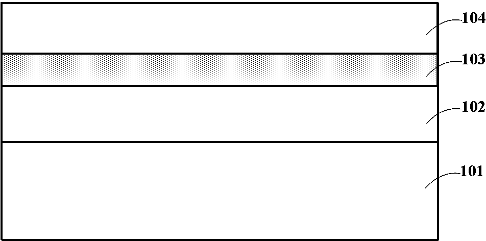
[0035] like figure 1 As shown, an N-type layer 102 , a light-emitting layer 103 and a P-type layer 104 are epitaxially grown sequentially on a sapphire substrate 101 by metal organic chemical vapor deposition (MOCVD).

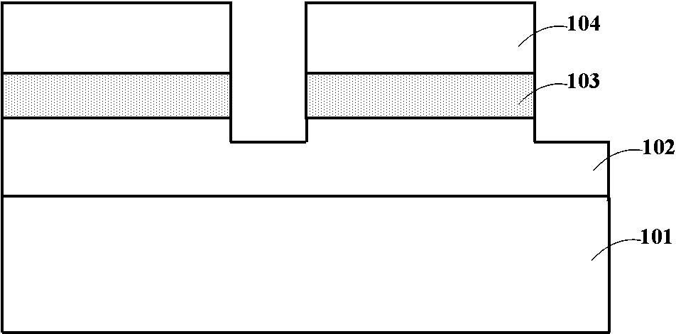
[0036] like figure 2 As shown, the N-type layer 102 is partially exposed by photolithography and etching techniques.

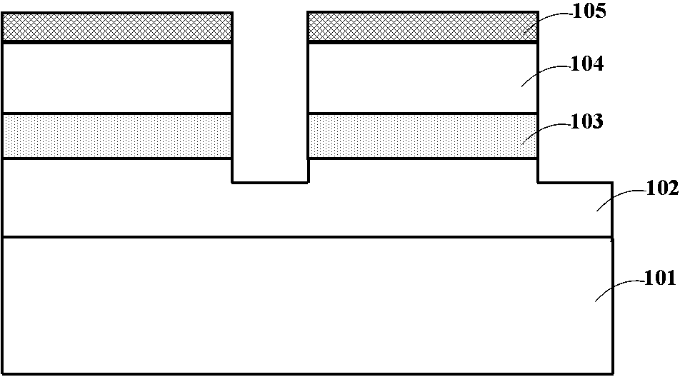
[0037] like image 3 As shown, an ITO transparent conductive layer 105 is formed on the surface of the epitaxial layer, that is, on the surface of the P-type layer 104 .

[0038] like Figure 4 As shown, a P electrode 106 and an N electrode 107 are respectively formed on the ITO transparent conductive layer 105 and the exposed N-type layer 102 by photolithography and etching techniques.

[0039] like Figure 5 As shown, the sapphire substrate 101 is thinned, and the thickness of the thinned sapphire substrate 101 ...

Embodiment 2

[0046]Different from Embodiment 1, in this embodiment, after the distributed Bragg reflection layer is vapor-deposited on the backside of the sapphire substrate and the U-shaped notch, the Al metal reflection layer is then sputtered to form an omnidirectional reflection layer. High thermal conductivity and high reflectivity, which is conducive to the further improvement of the light extraction efficiency of the LED chip and the improvement of the heat dissipation performance.


PUM


Abstract

The invention provides a manufacturing method for an LED chip by utilizing the laser scribing technology, the etching technology and the reflective layer back-plating technology. Two times of laser light are adopted for deflecting back scribing, so that scribing width and scribing depth are increased, and a U-shaped gap is formed; due to etching, scraps caused by laser scribing can be removed, and the surface of the U-shaped gap is more flat; a locally tilted side face is formed on a sapphire substrate through the U-shaped gap, after the side face and the obverse side of the substrate form a high-reflectance layer, rays emitted from a light-emitting layer can be reflected upward to a greater degree, and therefore the light-emitting efficiency of the LED chip is enhanced.

Description

technical field [0001] The invention relates to the field of semiconductor devices, in particular to a method for manufacturing light-emitting diode chips in combination with laser scribing, etching and back-plating reflective layer technologies. Background technique [0002] At present, blue-green LEDs suitable for commercial use are usually III-V compound semiconductor materials based on gallium nitride. Due to its unique bandgap range, excellent optical and electrical properties, and excellent physical and chemical properties, it can , violet, ultraviolet and white light-emitting diodes, short-wavelength laser diodes, ultraviolet detectors, power electronic devices and other optoelectronic devices and electronic devices, as well as semiconductor devices under special conditions, have been widely used. [0003] At present, the general process for preparing LED chips is: 1) GaN semiconductor layer is prepared by epitaxial growth on sapphire substrate; 2) P electrode and N e...

Claims


Application Information

Patent Timeline
Patent Type & Authority Applications(China)
IPC IPC(8): H01L33/00H01L33/60H01L33/64
CPCH01L33/0066H01L33/0075H01L2933/0058
Inventor 蔡家豪高维洋孟亚薇查劲松古静王印
Owner ANHUI SANAN OPTOELECTRONICS CO LTD
Why Eureka
Try Eureka