Preparation apparatus for diamond film and method for preparing diamond film by using apparatus
A diamond film, non-metal technology, applied in metal material coating process, gaseous chemical plating, coating and other directions, can solve the problems of diamond waste, different density distribution of active groups, poor uniformity of diamond film thickness, etc. , to achieve the effect of changing the density distribution and improving the uniformity of deposition
- Summary
- Abstract
- Description
- Claims
- Application Information
AI Technical Summary
Problems solved by technology
Method used
Image
Examples
Embodiment 1
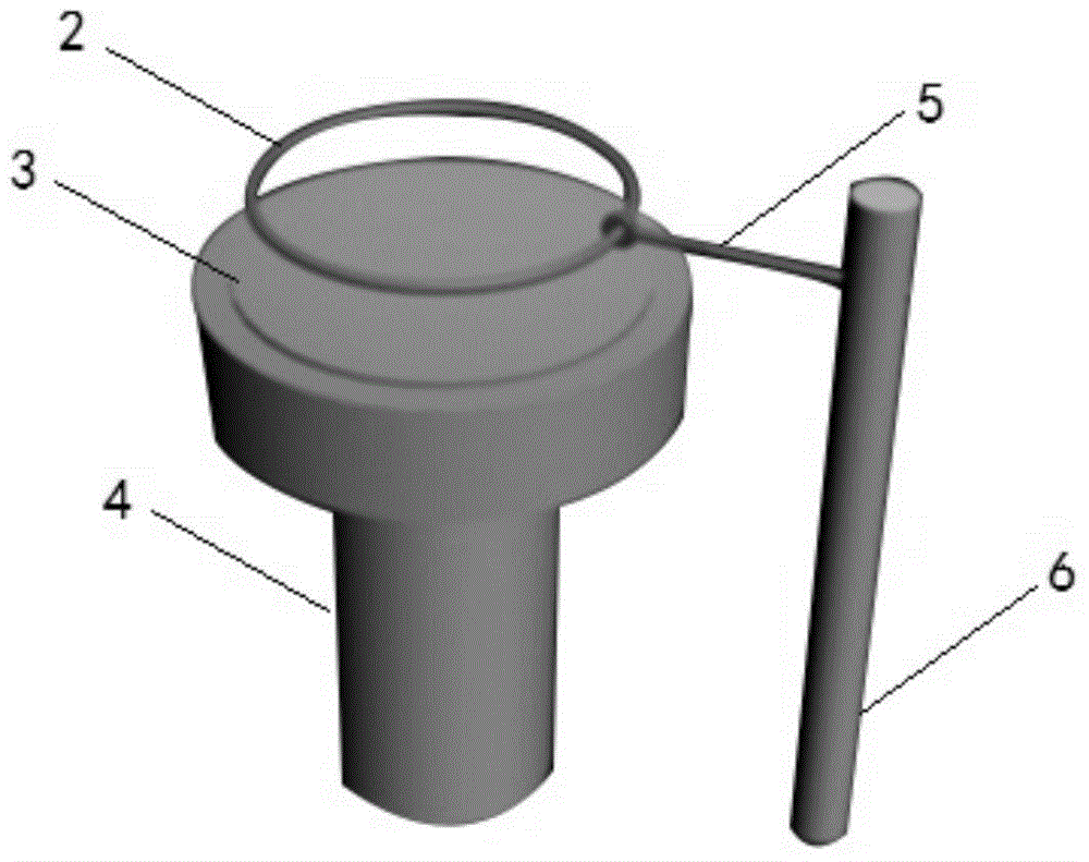
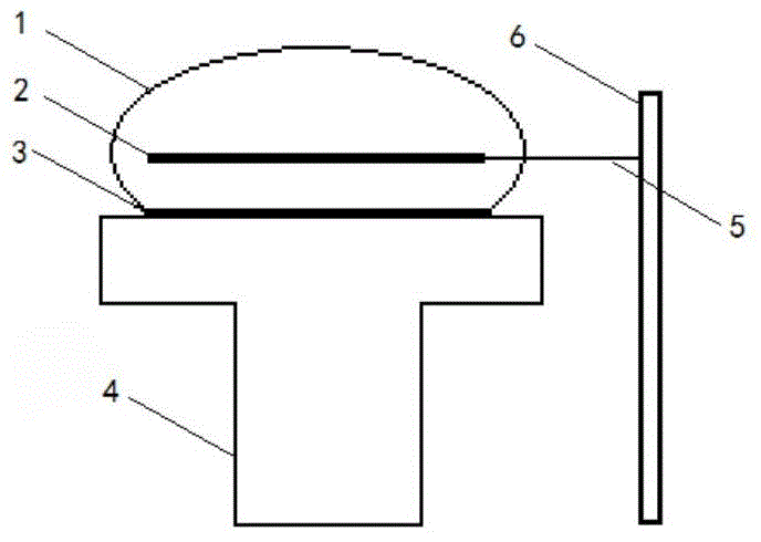
[0030] Surface carbonization treatment of high-temperature-resistant metal rings: select tantalum wires with a diameter of 1.0mm to make high-temperature-resistant metal rings with a diameter of 10mm, and place the tantalum wires in the plasma reaction chamber for surface carbonization treatment {microwave power 800W, working pressure 8.8kPa , methane flow 10sccm (standard cubic centimeter per minute), hydrogen flow 200sccm, time 15min}. Place the high-temperature-resistant metal ring after surface carbonization treatment horizontally at a vertical height of 5 mm from the spin-rotating substrate table. The schematic diagram of its installation position is as follows: figure 1 shown. An alumina support 6 is set up around the self-rotating substrate table 4, and the high temperature resistant metal ring 2 is fixedly connected to the alumina support 6 through a tungsten wire 5.
[0031] The diamond film was deposited on a P-type (100) single crystal silicon wafer with a diamete...
Embodiment 2
[0038] Surface carbonization treatment of high-temperature-resistant metal rings: tantalum wires with a diameter of 1.0 mm were selected to manufacture high-temperature-resistant metal rings with a diameter of 15 mm, and the surface carbonization treatment was carried out on the tantalum wires by the same method as in Example 1. Place the high-temperature-resistant metal ring after surface carbonization treatment horizontally at a vertical height of 7mm from the rotating substrate table.
[0039] The diamond film was deposited on a P-type (100) single crystal silicon wafer with a diameter of 20 mm and a thickness of 1 mm as a substrate. The surface of the substrate was degreased using the same method as in Example 1.
[0040] The diamond film was prepared using the following steps:
[0041] (1) Put the above-mentioned substrate degreased on the surface on the spin-rotating substrate stage in the plasma reaction chamber, and draw a background vacuum to the plasma reaction cham...
Embodiment 3
[0046] Surface carbonization treatment of high-temperature-resistant metal ring: Thin tantalum wire was selected to manufacture a high-temperature-resistant metal ring with a diameter of 20 mm, and the surface carbonization treatment was carried out on the tantalum wire by the same method as in Example 1. Place the high-temperature-resistant metal ring after surface carbonization treatment horizontally at a vertical height of 9 mm from the spin-rotating substrate table.
[0047] The diamond film was deposited on a P-type (100) single crystal silicon wafer with a diameter of 20 mm and a thickness of 1 mm as a substrate. The surface of the substrate was degreased using the same method as in Example 1.
[0048] The diamond film was prepared using the following steps:
[0049] (1) Put the above-mentioned substrate degreased on the surface on the spin-rotating substrate stage in the plasma reaction chamber, and draw a background vacuum to the plasma reaction chamber for 10 -2 Pa,...
PUM
| Property | Measurement | Unit |
|---|---|---|
| diameter | aaaaa | aaaaa |
| thickness | aaaaa | aaaaa |
| diameter | aaaaa | aaaaa |
Abstract
Description
Claims
Application Information
 - R&D
- Intellectual Property
- Life Sciences
- Materials
- Tech Scout
- Unparalleled Data Quality
- Higher Quality Content
- 60% Fewer Hallucinations
Browse by: Latest US Patents, China's latest patents, Technical Efficacy Thesaurus, Application Domain, Technology Topic, Popular Technical Reports.
© 2025 PatSnap. All rights reserved.Legal|Privacy policy|Modern Slavery Act Transparency Statement|Sitemap|About US| Contact US: help@patsnap.com


