Method for manufacturing diamond device
A diamond and device technology, applied in the field of semiconductor devices, can solve the problems of increased gate-source and gate-drain resistance, decreased transistor frequency performance, etc., and achieve the effects of reducing ohmic contact resistance, improving performance and simple preparation method
- Summary
- Abstract
- Description
- Claims
- Application Information
AI Technical Summary
Problems solved by technology
Method used
Image

Examples
Embodiment 1
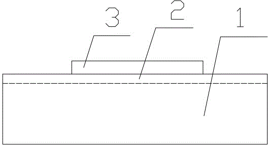
[0029] In the first step, the active area on the surface of the diamond semiconductor material with a p-type conductive channel is covered with photoresist;
[0030] The second step is to use the photoresist as a mask to etch the diamond conductive channel outside the active area with oxygen plasma for 10 minutes to remove the conductive channel;
[0031] The third step is to cover the photoresist outside the source and drain positions;
[0032] The fourth step is to transfer and cover the double-layer graphene grown on the Ni substrate by CVD method on the diamond surface;
[0033] The fifth step is to deposit ohmic contact metal Ti / Au 10 nm / 200nm on the graphene;
[0034] The sixth step is peeling off to form source and drain;
[0035] In the seventh step, electron beam lithography prepares a T-shaped grid with a grid length of 100 nm, evaporates 200 nm of Al grid metal, and peels off to form a diamond device.
Embodiment 2
[0037] In the first step, the active area on the surface of the diamond semiconductor material with an n-type conductive channel is covered with photoresist;
[0038] The second step is to use the photoresist as a mask to etch the diamond conductive channel outside the active area with oxygen plasma for 10 minutes to remove the conductive channel;
[0039] The third step is to cover the photoresist outside the source and drain positions;
[0040] The fourth step is to transfer and cover the double-layer graphene grown on the Ni substrate by CVD method on the diamond surface;
[0041] The fifth step is to deposit ohmic contact metal Ti / Au 10 nm / 200nm on the graphene;
[0042] The sixth step is peeling off to form source and drain;
[0043] In the seventh step, electron beam lithography prepares a T-shaped grid with a grid length of 100 nm, evaporates 200 nm of Al grid metal, and peels off to form a diamond device.
Embodiment 3
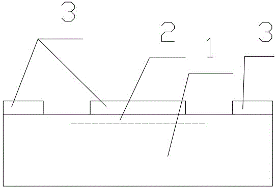
[0045] In the first step, the active area on the surface of the diamond semiconductor material with a p-type conductive channel is covered with photoresist;
[0046] The second step is to use the photoresist as a mask to etch the diamond conductive channel outside the active area with oxygen plasma for 10 minutes to remove the conductive channel;
[0047] The third step is to cover the photoresist outside the source and drain positions;
[0048] The fourth step is to transfer and cover the graphene grown on the Cu substrate by CVD method on the diamond surface;
[0049] The fifth step is to deposit ohmic contact metal Au 200nm on the graphene;
[0050] The sixth step is peeling off to form source and drain;
[0051] In the seventh step, electron beam lithography prepares a T-shaped grid with a grid length of 100 nm, evaporates 200 nm of Al grid metal, and peels off to form a diamond device.
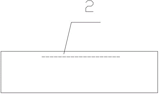
[0052] In the present invention, a graphene layer is inserted between the diamond ...
PUM
 Abstract
Description
Claims
Application Information
 - R&D
- Intellectual Property
- Life Sciences
- Materials
- Tech Scout
- Unparalleled Data Quality
- Higher Quality Content
- 60% Fewer Hallucinations
Browse by: Latest US Patents, China's latest patents, Technical Efficacy Thesaurus, Application Domain, Technology Topic, Popular Technical Reports.
© 2025 PatSnap. All rights reserved.Legal|Privacy policy|Modern Slavery Act Transparency Statement|Sitemap|About US| Contact US: help@patsnap.com