Transistor and forming method thereof

A transistor and semiconductor technology, applied in the manufacture of transistors, semiconductor devices, semiconductor/solid-state devices, etc., can solve the problems of high dielectric constant, affect the performance of transistors, reduce the effect of stress in the channel region, etc., and achieve the effect of increasing the size of the stress.

Active Publication Date: 2014-07-09
SEMICON MFG INT (SHANGHAI) CORP
View PDF5 Cites 17 Cited by
  • Summary
  • Abstract
  • Description
  • Claims
  • Application Information

AI Technical Summary

Problems solved by technology

[0009] In the prior art, three-layer sidewalls need to be formed on both sides of the gate structure, the process steps are complicated and the cost is high
And there are still silicon oxide spacers 132 and silicon nitride blocking spacers 131 between the stress layer and the gate structure formed last, and the silicon oxide spacers 132 will still reduce the stress effect of the stress layer 16 on the channel region
If the silicon oxide sidewall is to be removed, an additional etching process is required, increasing the process steps
Moreover, the dielectric constant of the silicon nitride blocking sidewalls 131 on both sides of the gate is relatively high, so that the parasitic capacitance around the gate structure of the formed transistor is relatively high, which affects the performance of the transistor.

Method used


Image

  • Transistor and forming method thereof
  • Transistor and forming method thereof
  • Transistor and forming method thereof

Examples


Embodiment Construction

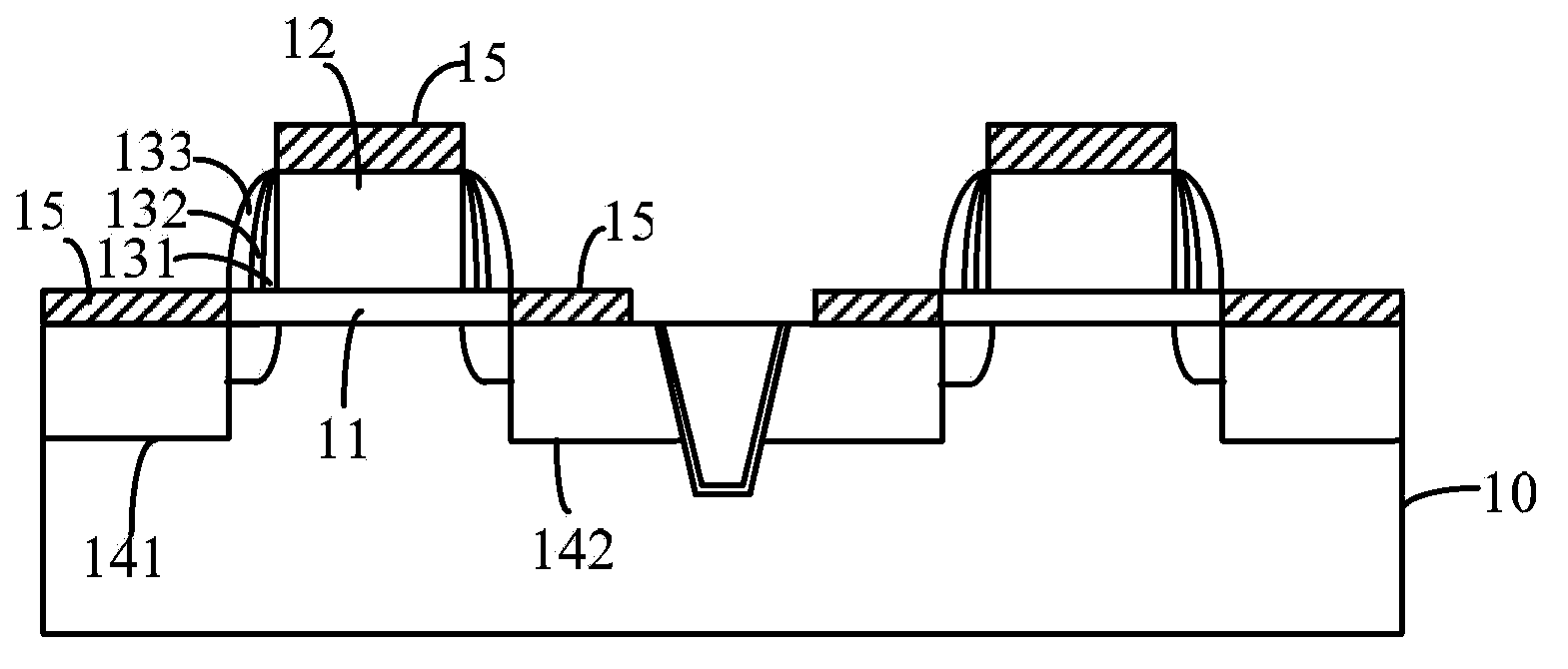
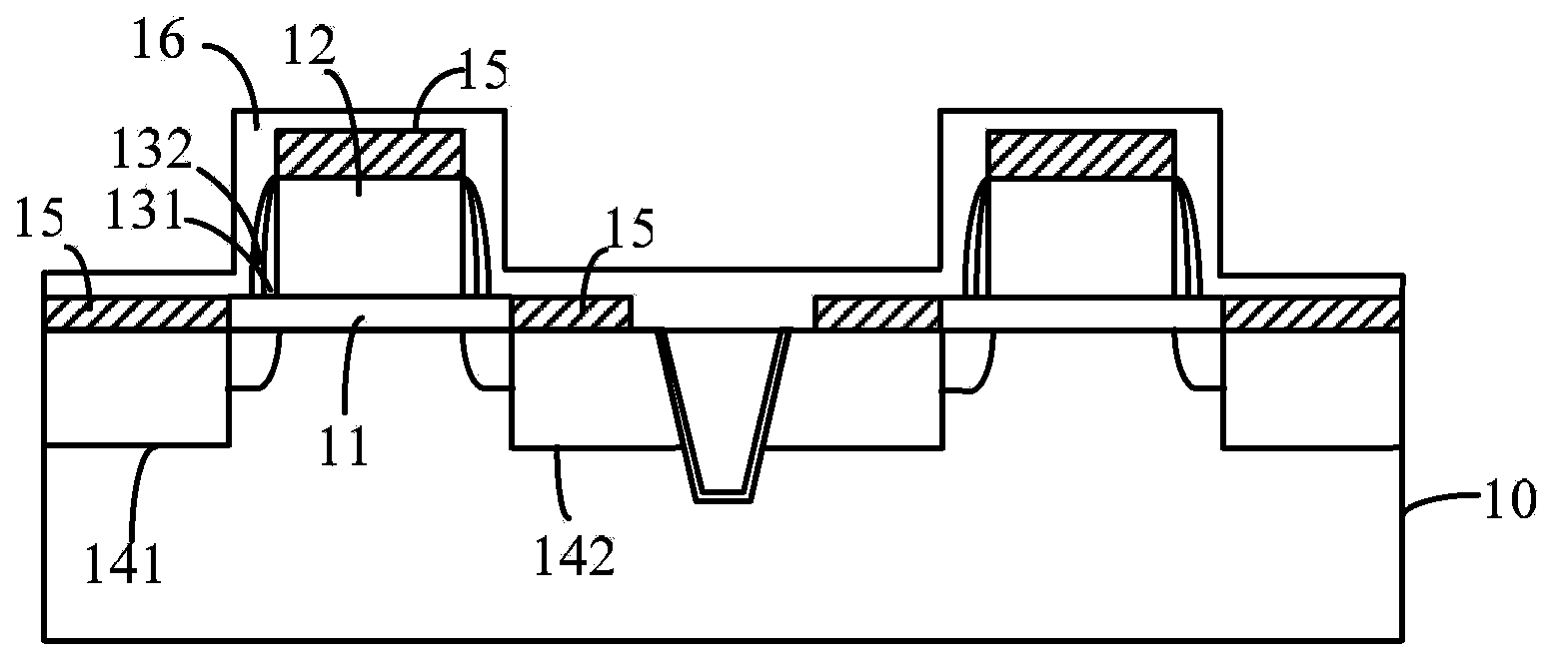
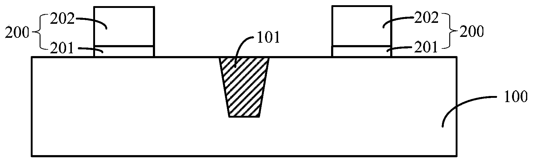
[0040] As mentioned in the background, the method for forming a transistor in the prior art needs to form three layers of sidewalls on both sides of the gate structure of the transistor, the steps are complicated, and the process cost is high. Moreover, the dielectric constant of the silicon nitride sidewall is relatively high, so that the parasitic capacitance around the gate structure of the formed transistor is relatively high, which affects the performance of the transistor.

[0041] In the method for forming a transistor proposed by the present invention, a first side wall and a second side wall are formed on both sides of the gate structure, the first side wall is a doped silicon nitride layer, and then a source electrode, a drain electrode, and a source electrode are formed. The metal silicide layer on the surface of the electrode and the drain, and then remove the second side wall to form a stress layer. Removing the second sidewall can reduce the distance between the ...


PUM


Abstract

The invention provides a transistor and a forming method of the transistor. The forming method of the transistor comprises the steps that a semiconductor substrate is provided, wherein an isolation structure is arranged in the semiconductor substrate, gate structures are arranged on the surfaces of the portions, on the two sides of the isolation structure, of the semiconductor substrate, and each gate structure comprises a gate dielectric layer on the surface of the semiconductor substrate and a gate electrode located on the surface of the gate dielectric layer; first side walls are formed on the two sides of the gate structure, wherein the first side walls are doped silicon nitride layers; second side walls are formed on the surfaces of the first side walls, and the etching rate of each second side wall is larger than the etching rate of each first side wall; a source electrode and a drain electrode are formed in the portions, located on the two sides of the gate structures, of the semiconductor substrate; metal silicide layers are formed on the surface of the source electrode and on the surface of the drain electrode; the second side walls are eliminated; a stress layer is formed on the surface of the semiconductor substrate. By the adoption of the forming method of the transistor, the stray capacitance on the two sides of the gate structures of the transistor can be reduced, and the stress borne by the trench area of the transistor is increased.

Description

technical field [0001] The invention relates to the technical field of semiconductors, in particular to a transistor and a forming method thereof. Background technique [0002] With the rapid development of semiconductor manufacturing technology, in order to achieve faster computing speed, larger data storage capacity and more functions of semiconductor devices, semiconductor chips are developing towards higher integration. The higher the integration degree of the semiconductor chip, the smaller the feature size (CD, Critical Dimension) of the semiconductor device. At present, the feature size of semiconductor devices is gradually shrinking, and stress strain technology (stress strain technology), such as stress proximate technology (SPT), is required in the manufacture of semiconductor devices. [0003] Figure 1 to Figure 2 It is a schematic cross-sectional structure diagram of a transistor manufacturing method using stress proximity technology in the prior art. [0004]...

Claims


Application Information

Patent Timeline
Patent Type & Authority Applications(China)
IPC IPC(8): H01L21/336H01L29/78H01L29/06
CPCH01L21/02167H01L21/0217H01L21/022H01L21/02211H01L21/02263H01L21/0228H01L21/31111H01L21/823418H01L21/823468H01L21/823814H01L21/823864H01L29/665H01L29/6653H01L29/6656H01L29/6659H01L29/7843H01L29/7833H01L29/7848H01L29/165
Inventor 何有丰何永根
Owner SEMICON MFG INT (SHANGHAI) CORP
Why Eureka
Try Eureka