
Multi-beam type single-mass in-plane biaxial acceleration sensor chip and preparation method thereof

A biaxial acceleration and sensor chip technology, applied in the direction of acceleration measurement using inertial force, can solve the problems of being easily affected by parasitic capacitance, narrow frequency response range, and low sensitivity, so as to improve dynamic performance and application range, reduce Interference of cross-sensitivity, effect of alleviating contradictory relationship

Active Publication Date: 2019-10-11
XI AN JIAOTONG UNIV
View PDF15 Cites 0 Cited by
  • Summary
  • Abstract
  • Description
  • Claims
  • Application Information

AI Technical Summary

Problems solved by technology

Acceleration sensors with different sensitivity principles have different advantages and disadvantages. For example, although piezoelectric acceleration sensors have been used maturely, they are limited by their sensitivity principles. Piezoelectric sensors cannot measure static acceleration, and the output charge signal needs subsequent assistance. circuit, it is not easy to realize the integrated design of sensitive chips and subsequent circuits; capacitive acceleration sensors have the advantages of high sensitivity, small temperature drift, and low power consumption, but have large input impedance and are easily affected by parasitic capacitance. Sensitive; piezoresistive acceleration sensor is susceptible to temperature, but it has a wide measurement range, can measure static and dynamic signals, has good dynamic response characteristics, and simple post-processing circuit
[0003] The commonly used structures of piezoresistive acceleration sensors include single cantilever beam, double cantilever beam, double-end fixed beam, four-sided four-fixed beam and other structures. These structures all adopt the beam-island structure, and the mass block swings freely in a fixed direction. , in which the single cantilever beam and the double cantilever beam have high sensitivity, but the natural frequency is low and the frequency response range is narrow.
[0004] With the development of science and technology, the current piezoresistive acceleration sensors have been difficult to meet the requirements of high sensitivity, high natural frequency and low cross-sensitivity in different fields, such as automotive intelligent detection, high-speed precision machine tools, fault diagnosis and monitoring of high-speed moving parts, electronic Vibration control of components, etc. However, for traditional piezoresistive acceleration sensors, their natural frequency and sensitivity are mutually restricted. This restrictive relationship brings a series of difficulties to dynamic acceleration measurement, and it is easy to be distorted during measurement. Therefore, research can alleviate the natural frequency. The acceleration sensor with the contradictory relationship between sensitivity and sensitivity is of great significance to reduce the influence of cross sensitivity and solve the problem of high sensitivity and high frequency response measurement of acceleration.

Method used


Image

  • Multi-beam type single-mass in-plane biaxial acceleration sensor chip and preparation method thereof
  • Multi-beam type single-mass in-plane biaxial acceleration sensor chip and preparation method thereof
  • Multi-beam type single-mass in-plane biaxial acceleration sensor chip and preparation method thereof

Examples


Embodiment

[0070] The method for preparing the acceleration sensor chip of the present embodiment comprises the following steps, referring to Figure 6 to Figure 8 :

[0071] Step 1), use the HF solution with a volume concentration of 49% to clean the SOI silicon chip of the N-type (100) crystal plane; the structure of the SOI silicon chip from top to bottom is: The layer 14 and the lower layer of single crystal silicon 15 have a thickness of 10 μm, 1 μm and 304 μm in sequence, wherein the buried silicon dioxide layer 14 separates the upper layer of single crystal silicon 13 from the lower layer of single crystal silicon 15;

[0072] Step 2), then carry out high-temperature oxidation on the SOI silicon wafer, the oxidation temperature is 900-1200 ° C, and form a silicon dioxide layer 10 on the front and back sides of the SOI silicon wafer, and then use a P-varistor plate to oxidize the upper layer single crystal The silicon dioxide layer 10 formed on the surface of the silicon 13 is pho...


PUM


Abstract

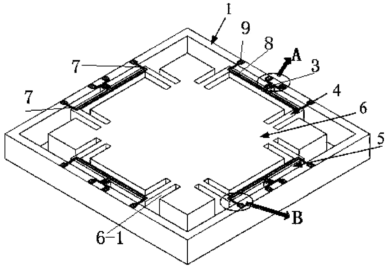
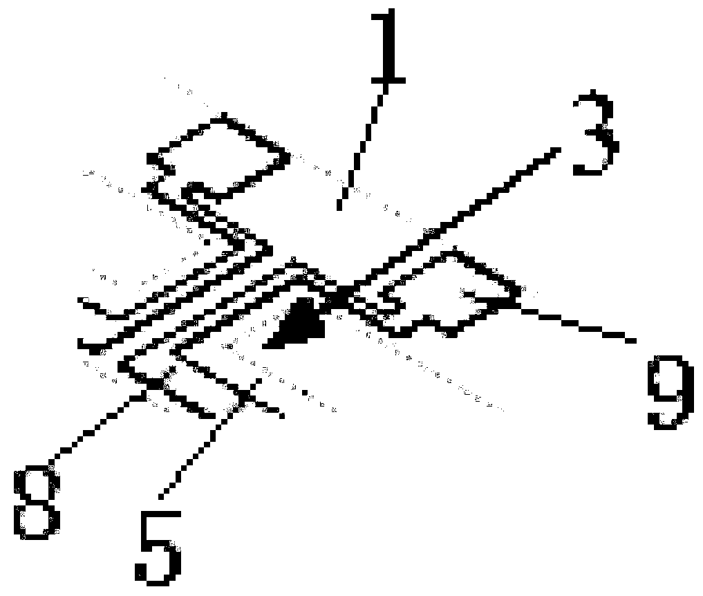
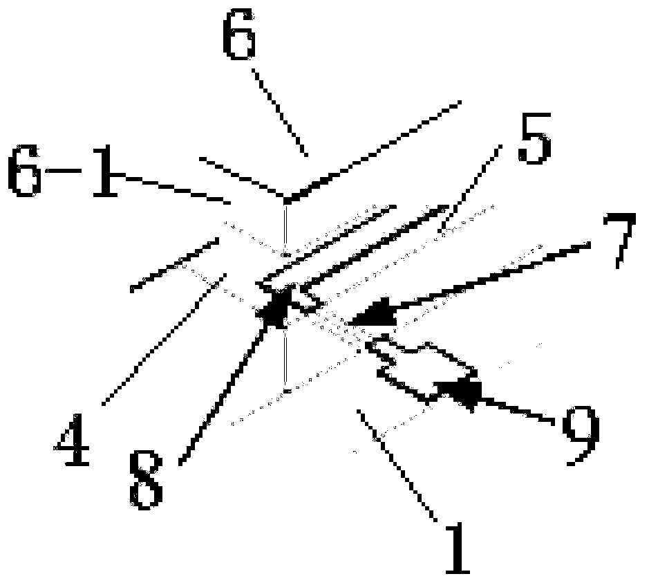
The present invention discloses a multi-beam type single-mass block in-plane biaxial acceleration sensor chip and a preparation method thereof. The sensor chip adopts an SOI silicon slice to manufacture, and comprises a chip outer frame, a master supporting beam, a connecting beam, a slave supporting beam, sensitive piezoresistive micro-beams, a mass block, metal lead wires and pads. One end of the master supporting beam is fixed to the chip outer frame, and the other end is connected with the connecting beam. The other end of the connecting beam is connected with the slave supporting beam, and the other end of the slave supporting beam is connected with the mass block. The eight sensitive piezoresistive micro-beams in the chip are located in the gaps between the chip outer frame and the connecting beam, every two sensitive piezoresistive micro-beams are distributed at the two sides of the master supporting beam symmetrically, one ends of the sensitive piezoresistive micro-beams are fixed to the chip outer frame, and the other ends are connected with the connecting beam. The piezoresistors on the eight sensitive piezoresistive micro-beams are connected via the metal lead wires andthe sixteen pads and form a Wheastone full-bridge circuit. The sensor chip of the present invention can realize the measurement of the acceleration less than 100g, has an inherent frequency more than40 kHz, and satisfies the high-frequency low-g value acceleration dynamic measurement requirement.

Description

technical field [0001] The invention belongs to the field of measurement of micromechanical electronic sensors, and in particular relates to a multi-beam type single-mass block in-plane biaxial acceleration sensor chip and a preparation method thereof. Background technique [0002] With the development of Micro Electro Mechanical Systems (MEMS) technology, acceleration sensors based on different principles have been widely used, such as piezoresistive, capacitive, electromagnetic, piezoelectric, resonator, Fiber optic type and thermocouple type, etc. Acceleration sensors with different sensitivity principles have different advantages and disadvantages. For example, although piezoelectric acceleration sensors have been used maturely, they are limited by their sensitivity principles. Piezoelectric sensors cannot measure static acceleration, and the output charge signal needs subsequent assistance. circuit, it is not easy to realize the integrated design of sensitive chips and...

Claims


Application Information

Patent Timeline
Patent Type & Authority Patents(China)
IPC IPC(8): G01P15/12
Inventor 赵立波贾琛蒋维乐于明智李支康王久洪赵玉龙蒋庄德
Owner XI AN JIAOTONG UNIV
Learn More