Quick counting and monitoring method of silicon substrate chip dislocation defects

A chip, silicon-based technology, applied in the field of rapid statistical monitoring of dislocation defects in silicon-based chips, can solve the problems of long time consumption, small observable area, low overall efficiency, etc. The effect of reducing labor costs

Active Publication Date: 2014-07-09
SHANGHAI HUAHONG GRACE SEMICON MFG CORP
View PDF7 Cites 6 Cited by
  • Summary
  • Abstract
  • Description
  • Claims
  • Application Information

AI Technical Summary

Problems solved by technology

[0008] 1. It takes a long time, and the preparation of the most complex single sample is calculated in hours
[0009] 2. The observable area is small. The length of a single sample is usually about 10 microns, and the depth is 2-4 microns. The thickn

Method used


Image

  • Quick counting and monitoring method of silicon substrate chip dislocation defects
  • Quick counting and monitoring method of silicon substrate chip dislocation defects
  • Quick counting and monitoring method of silicon substrate chip dislocation defects

Examples


Embodiment Construction

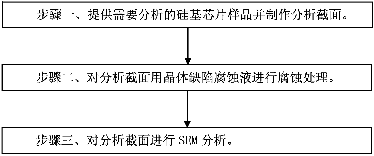
[0042] Such as figure 1 As shown, it is a flow chart of the method of the embodiment of the present invention; the rapid statistical monitoring method of the silicon-based chip dislocation defect in the embodiment of the present invention includes the following steps:

[0043] Step 1. Provide a silicon-based chip sample to be analyzed, and make an analysis section of the silicon-based chip sample that needs to be analyzed. The crystal plane index of the analysis section belongs to the {110} crystal plane family.

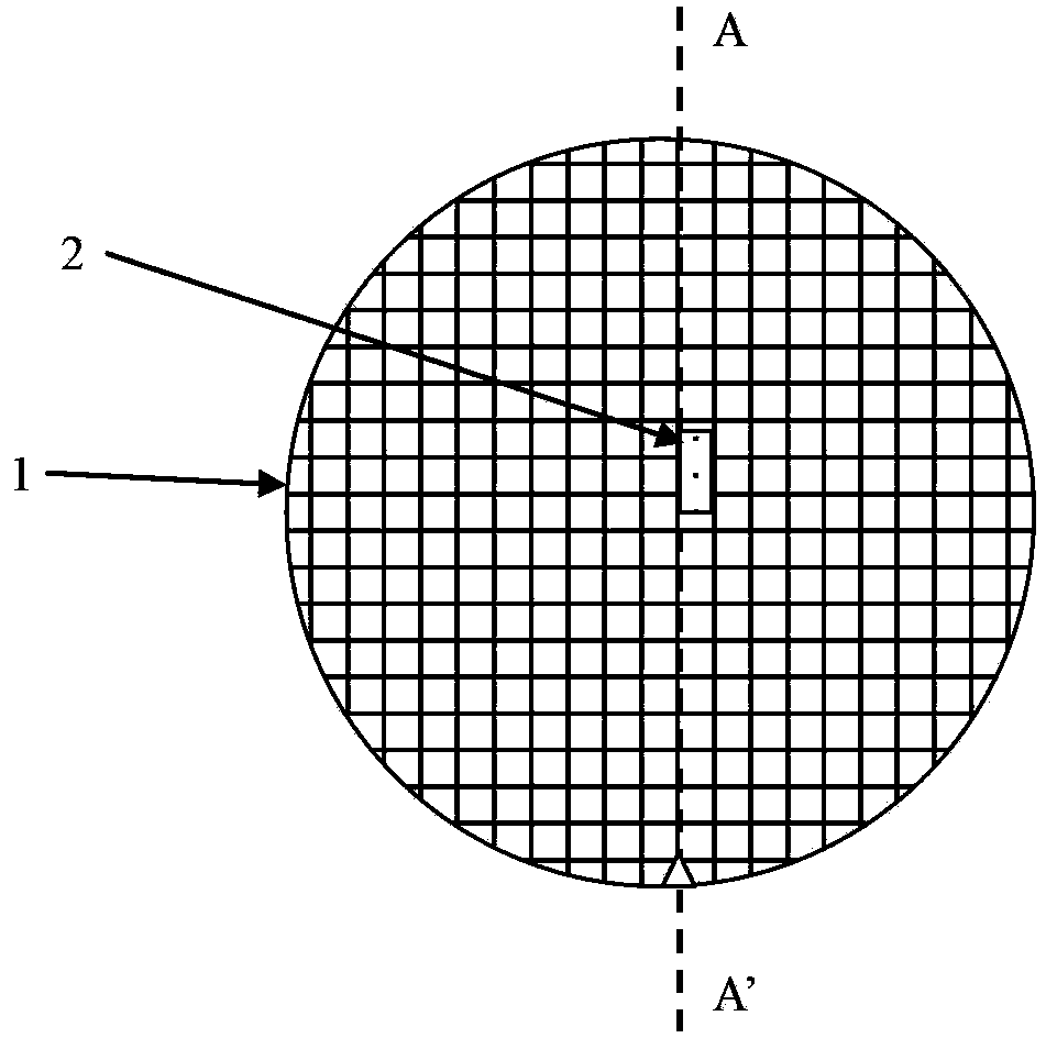
[0044] Such as figure 2 As shown, it is a schematic diagram of the preparation of the analysis section of the wafer-level sample in the method of the embodiment of the present invention; for silicon wafers. The crystal plane index of the profile of the dotted line AA’ belongs to the {110} crystal plane family, so it is only necessary to follow figure 2 The analysis section can be formed by manually splitting in the direction of the dotted line AA' in .

[0045]...


PUM


Abstract

The invention discloses a quick counting and monitoring method of silicon substrate chip dislocation defects. The method comprises the steps of providing a silicon substrate chip sample needing analysis and manufacturing an analysis section. The analysis section is subjected to corrosion processing through crystal defect corrosive liquid, and is subjected to SEM analysis. The method increases the observation range of the dislocation defects on a silicon substrate, and can improve analysis speed of the dislocation defects, improve dislocation monitoring and analysis efficiency and lower cost.

Description

technical field [0001] The invention relates to a semiconductor integrated circuit manufacturing process method, in particular to a fast statistical monitoring method for silicon-based chip dislocation defects. Background technique [0002] There are two commonly used analysis methods for dislocation defects in silicon-based chips: [0003] The first method is to first prepare a sample with a thickness of about 100nm at a fixed point using a focused ion beam electron microscope (Focused Ion Beam, FIB), and then use a transmission electron microscope (Transmission electron microscope, TEM) to observe the structure of the prepared sample. [0004] The second method is to first prepare a thin slice sample with a thickness of about 100nm by using an ion thinner, and then use TEM to observe the structure of the prepared sample. [0005] The FIB sample preparation in the existing first method is: [0006] Use the focused gallium positive ion beam as the incident particle (or pri...

Claims


Application Information

Patent Timeline
IPC IPC(8): H01L21/66
CPCH01L22/12H01L22/20
Inventor 刘苏南蔡妮妮赖华平廖炳隆
Owner SHANGHAI HUAHONG GRACE SEMICON MFG CORP
Why Eureka
Try Eureka