Method for encapsulating CZT pixel detector
A packaging method and detector technology, applied in radiation control devices and other directions, can solve problems such as poor practicability, and achieve the effects of strong practicability, uniform size, and good electrical conductivity
- Summary
- Abstract
- Description
- Claims
- Application Information
AI Technical Summary
Problems solved by technology
Method used
Image
Examples
Embodiment Construction
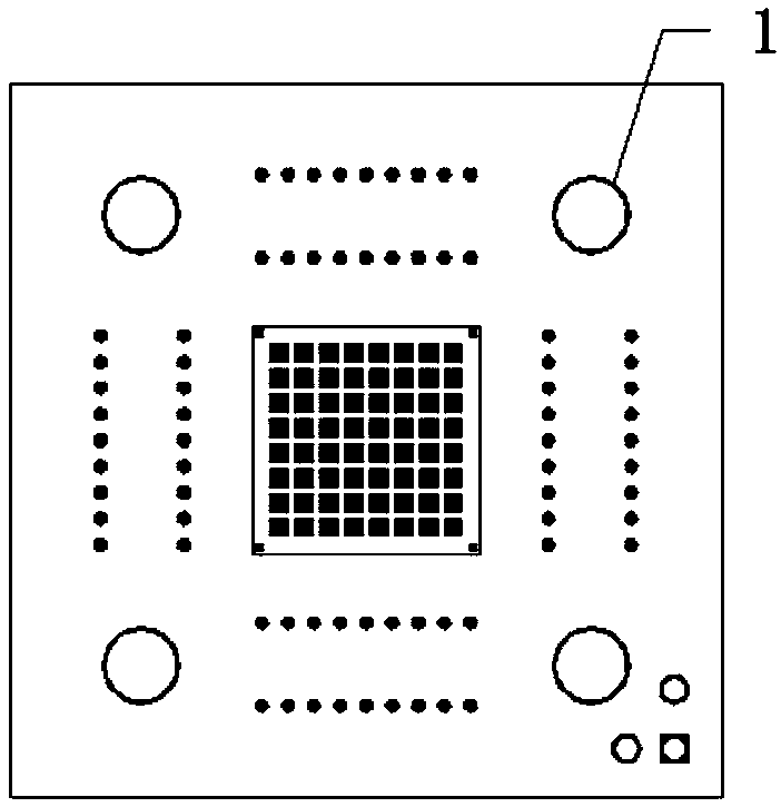
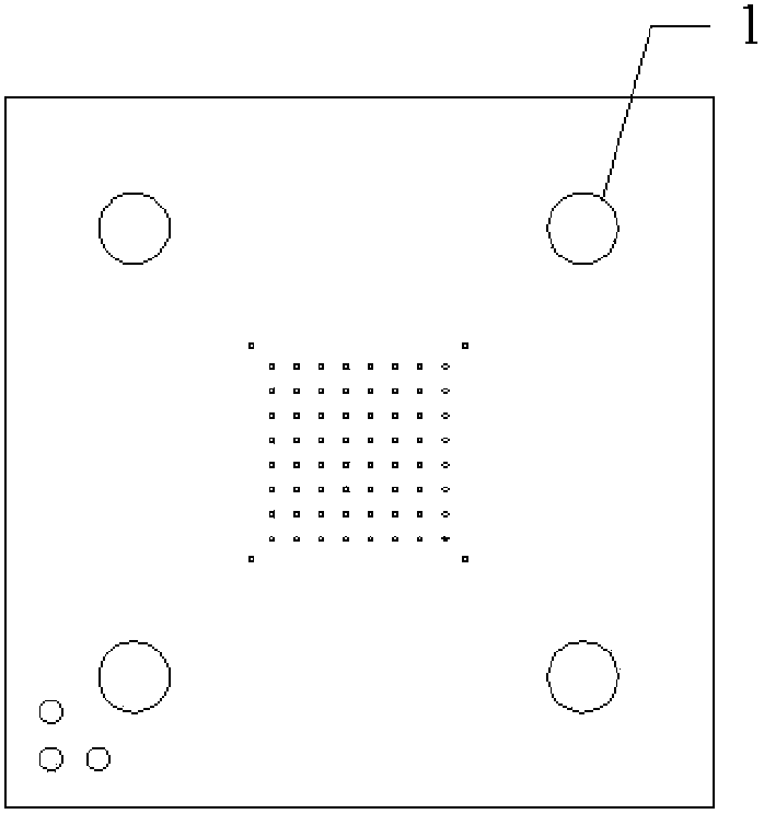
[0020] The following examples refer to Figure 1-5 .
[0021] The crystal used in the CZT pixel detector is a CZT crystal ingot grown by the vertical Bridgman method, cut into 10×10×2㎜ 3 single crystal, and prepared 8×8 pixel electrodes. Subsequently, the CZT pixel detector and the PCB board flip are connected by screen printing through conductive silver glue. The thickness of the stainless steel mesh used for screen printing is 100 μm, the diameter of the round hole is 200 μm, and the leakage current test system is used for I-V testing.
[0022] The first step: use the CZT crystal ingot grown by the vertical Bridgman method, cut the single crystal part into 10×10×2㎜3 wafers, polish all sides of the wafer on 5000# sandpaper, and then use MgO to suspend The silicon sol is used for rough polishing, the silica sol is used for mechanical chemical polishing, the processed wafer is carefully cleaned with acetone, and it is etched with bromomethanol to remove the mechanical damage ...
PUM
| Property | Measurement | Unit |
|---|---|---|
| Thickness | aaaaa | aaaaa |
| Diameter | aaaaa | aaaaa |
Abstract
Description
Claims
Application Information
 - R&D Engineer
- R&D Manager
- IP Professional
- Industry Leading Data Capabilities
- Powerful AI technology
- Patent DNA Extraction
Browse by: Latest US Patents, China's latest patents, Technical Efficacy Thesaurus, Application Domain, Technology Topic, Popular Technical Reports.
© 2024 PatSnap. All rights reserved.Legal|Privacy policy|Modern Slavery Act Transparency Statement|Sitemap|About US| Contact US: help@patsnap.com


