Method for manufacturing printed circuit board with conical optical waveguide

A technology of printed circuit board and tapered optical waveguide, which is applied in the direction of optical waveguide light guide, light guide, optics, etc., to achieve the effect of improving coupling efficiency, reducing coupling loss, and simple manufacturing process

Active Publication Date: 2014-07-16
SHANGHAI MEADVILLE SCI & TECH
View PDF6 Cites 4 Cited by
  • Summary
  • Abstract
  • Description
  • Claims
  • Application Information

AI Technical Summary

Problems solved by technology

The cross-section of the optical fiber corresponding to the coupling device is circular, and there are always different degrees of coupling loss when the rectangular optical waveguide of the same size is coupled with the circular optical fiber.

Method used


Image

  • Method for manufacturing printed circuit board with conical optical waveguide
  • Method for manufacturing printed circuit board with conical optical waveguide
  • Method for manufacturing printed circuit board with conical optical waveguide

Examples


Embodiment 1

[0030] see Figure 1 to Figure 8 , taking a four-layer copper layer + one optical waveguide layer as an example (two copper layers + one optical waveguide layer + two copper layers), the process flow is as follows:

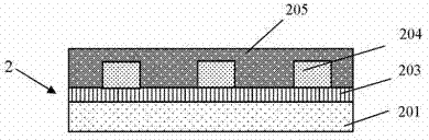
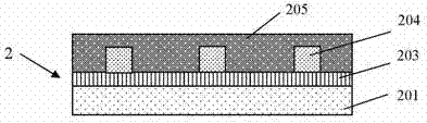
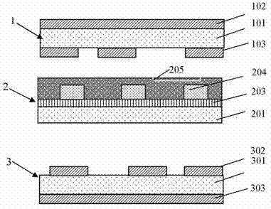
[0031] 1) Substrate production, 1, 2, and 3 are cut copper clad laminates, copper clad laminates 1 and 3 are used for the production of four copper layers, and the copper clad laminate 2 in the middle is used for the production of the optical waveguide layer. Among them, 101 is a dielectric layer, 102 and 103 are copper layers, see figure 1 ; The optical waveguide substrate 201 is a copper clad laminate with copper etched away, see figure 2 .

[0032] 2) Fabrication of the optical waveguide layer, including the lower cladding layer 203, the core layer 204, and the upper cladding layer 205, see image 3 , the specific production steps include film application, exposure, development, and baking. Wherein, the optical waveguide material used in the core layer and...

Embodiment 2

[0041] This embodiment is the manufacture of a six-layer PCB board with a tapered optical waveguide. Firstly, the manufacture of the inner substrate is completed through material cutting and pattern transfer of the core board, and then the manufacture of the optical waveguide is performed on the inner substrate. The optical waveguide is produced by coating, exposing, developing, and baking the optical waveguide wet film material. The cross-section of the input end of the tapered optical waveguide core layer is 70×70 μm, the cross-section of the output end is 30×30 μm, and the length of the optical waveguide is It is 50cm. Follow-up is completed through lamination, drilling, electroplating, graphic production, green oil, characters, chemical immersion silver, testing, milling shape, packaging, etc.

[0042] Table 1

[0043] Axial offset (μm)

[0044] -15

[0045] Table 2

[0046] Longitudinal offset (μm)

[0047] In summary, the printed circuit b...


PUM


Abstract

A method for manufacturing a printed circuit board with a conical optical waveguide includes the following steps that firstly, a substrate is manufactured, wherein the substrate is formed by a copper-clad plate, a medium layer is arranged in the middle of the copper-clad plate, and copper layers are arranged on the two sides of the copper-clad plate; secondly, an optical waveguide layer is manufactured, wherein an upper wrapper, a core layer and a lower wrapper are sequentially manufactured on the substrate, wherein the area of the cross section of the core layer of the optical waveguide gradually decreases in the optical signal propagation direction, the area of the cross section of the input end of the core layer of the optical waveguide is larger than the area of the cross section of the output end of the core layer, and then the conical optical waveguide is formed; thirdly, a matched printed circuit board is manufactured; fourthly, the printed circuit board and the substrate with the optical waveguide layer are laminated to form a mixed plate with the optical waveguide layer and the copper layers; fifthly, the mixed plate is subsequently machined through the drilling step, the electroplating step, the graph manufacturing step, the green oil coating step, the surface processing step, the cleaning step, the examining step, the cleaning step and the packaging step. According to the method, optical waveguide coupling loss of the circuit board can be effectively reduced, and the alignment tolerance of an optical fiber or the optical waveguide can be increased under the same coupling loss requirement.

Description

technical field [0001] The invention relates to the technical field of printed circuits, in particular to a method for manufacturing a printed circuit board containing a tapered optical waveguide. Background technique [0002] With the rapid development of high-speed information communication networks, the traditional electrical interconnection methods are increasingly unsuitable for high-speed information processing and transmission due to electromagnetic interference of metal wires, RC delay, and high transmission loss. In this context, a large number of companies have begun to study a new optical interconnection method. Optical interconnection replaces electrical interconnection and has obvious advantages. During high-speed transmission of optical interconnection, signal divergence is small, distortion is small, and loss is low, which can easily achieve and maintain good signal integrity. Nowadays, optical interconnection is widely used in the research of interconnection...

Claims


Application Information

Patent Timeline
Patent Type & Authority Applications(China)
IPC IPC(8): G02B6/13G02B6/136
Inventor 吴金华严惠娟朱龙秀
Owner SHANGHAI MEADVILLE SCI & TECH
Why Eureka
Try Eureka