Method for manufacturing surface plasmon polariton nanometer photonic device

A surface plasmon and nanophotonic technology, applied in the direction of optical waveguide and light guide, can solve the problems of complex preparation, high cost, large size of nanophotonic devices, etc., and achieve simple device preparation process, good grain characteristics and controllability, and process flow. simple effect

Active Publication Date: 2014-07-30
INST OF MICROELECTRONICS CHINESE ACAD OF SCI
View PDF3 Cites 4 Cited by
  • Summary
  • Abstract
  • Description
  • Claims
  • Application Information

AI Technical Summary

Problems solved by technology

[0009] In view of this, the main purpose of the present invention is to provide a method for preparing surface plasmon nanophotonic devices, so as to solve the problems of large size, complex preparation and high cost of current nanophotonic devices

Method used


Image

  • Method for manufacturing surface plasmon polariton nanometer photonic device

Examples


Embodiment

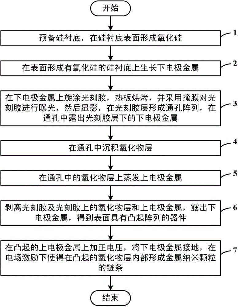
[0051] In this embodiment, a 2-inch silicon substrate is selected, the substrate dielectric layer is made of silicon oxide, the active electrode is made of silver (Ag), and the inert electrode is made of platinum (Pt). In this embodiment, a standard cleaning process is first performed on a 2-inch silicon substrate to remove surface oil and metal contamination. The cleaned silicon substrate is oxidized in a high-temperature oxidation furnace to form insulating silicon oxide on the surface, which is used as a substrate dielectric layer with a thickness of about 100 nanometers. On the silicon substrate formed with silicon oxide, electron beam evaporation forms the lower electrode metal platinum (Pt) with a thickness of 70 nanometers, and then spin-coats 9920 photoresist at a speed of 7000 revolutions per minute, spin coating for one minute, and the thickness is about 1.2 microns. Bake on a hot plate at 85°C for 4.5 minutes. Exposure adopts vacuum exposure mode, and the exposure t...


PUM

PropertyMeasurementUnit
thicknessaaaaaaaaaa
thicknessaaaaaaaaaa
thicknessaaaaaaaaaa

Abstract

The invention discloses a method for manufacturing a surface plasmon polariton nanometer photonic device. The method comprises the steps that a silicon substrate is prepared; lower electrode metal is grown on the silicon substrate with silicon oxide formed on the surface; the lower electrode metal is coated with a photoresist layer in a spinning mode, a hot plate is roasted, the photoresist layer is exposed through a mask and then is developed, a through hole array is formed on the photoresist layer, and the lower electrode metal below the photoresist layer is exposed out of the through hole; an oxide layer is deposited in the through hole; upper electrode metal is evaporated in the through hole; the photoresist layer, and the oxide layer and the upper electrode metal on the photoresist layer are peeled off, the lower electrode metal is exposed, and a device with a protruding array on the surface is obtained; positive voltage is added on the protruding upper electrode metal, the lower electrode metal is grounded, a metal nano-particle chain is formed inside the protruding oxide layer under excitation of an electric field, and the surface plasmon polariton nanometer photonic device is obtained. By the utilization of the method for manufacturing the surface plasmon polariton nanometer photonic device, the problems that an existing nanometer photonic device is large in size, complex in manufacturing and high in cost are solved.

Description

technical field [0001] The invention relates to the technical field of nano-photonic devices and nano-processing, in particular to a method for preparing surface plasmon nano-photonic devices. Background technique [0002] With the continuous development of micro-nano processing technology, the size of the device is greatly reduced. Due to the influence of the diffraction effect, the traditional spot size or the diameter of the beam is generally limited to the scale range of the wavelength order. Advances in micro-nano-fabrication technology and integrated optics have led to the continuous miniaturization of optical devices, approaching the diffraction limit of light. How to obtain various high-efficiency optoelectronic devices that break through the diffraction limit is the basis for realizing nano-all-optical integration, and it is also an important research hotspot in the field of micro-nano optics. When the light wave (electromagnetic wave) is incident on the interface ...

Claims


Application Information

Patent Timeline
Patent Type & Authority Applications(China)
IPC IPC(8): G02B6/13
Inventor 孙海涛刘琦吕杭炳龙世兵刘明
Owner INST OF MICROELECTRONICS CHINESE ACAD OF SCI
Why Eureka
Try Eureka