

Adhesive tape encapsulating structure of organic light emitting diode
A technology of light-emitting diodes and packaging structures, which is applied in the manufacturing of electrical components, electric solid-state devices, semiconductor/solid-state devices, etc., can solve the problems of high device cost, complex process, expensive packaging equipment and related materials, etc. Cost, simple process, and the effect of increasing the speed of production
- Summary
- Abstract
- Description
- Claims
- Application Information
AI Technical Summary
Problems solved by technology
Method used
Image

Examples
Embodiment 1
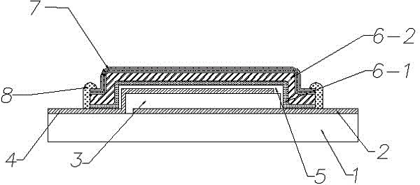
[0024] Such as figure 1 As shown, a tape encapsulation structure of an organic light emitting diode has a front electrode 2 with ITO on the glass substrate 1, and includes an organic hole injection layer, an organic hole transport layer, an organic light emitting layer, an organic electron transport layer and The organic layer 3 of the organic electron injection layer, the metal aluminum rear electrode 4 and the protective layer 5 of organic materials are used for tape packaging of the bottom-emitting organic light-emitting diode OLED of the glass substrate 1, and the tape 6 used for the tape packaging of the OLED is a A kind of adhesive tape which is coated with a layer of self-adhesive layer 6-1 under the polyimide flexible film tape 6-2 which has better resistance to the passage of water vapor and oxygen, and a gas barrier layer composed of multi-layer films on the adhesive tape 7 It is composed of a multi-layered thin film consisting of a silicon nitride layer, an aluminum...
Embodiment 2
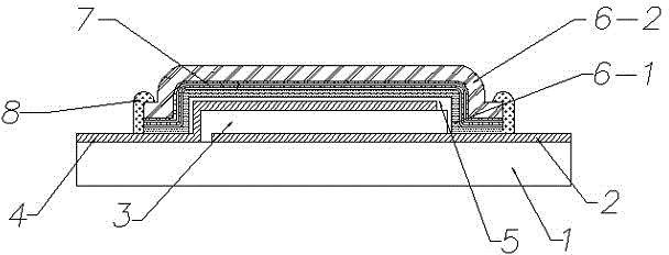
[0026] Such as figure 2 As shown, the difference from Embodiment 1 is that the gas barrier layer 7 here is between the polyimide flexible film tape 6-2 and the self-adhesive layer 6-1. During the production process of the tape 6, the gas barrier layer 7 is prepared under the polyimide flexible film tape 6-2, and then the self-adhesive layer 6-1 is coated.
Embodiment 3
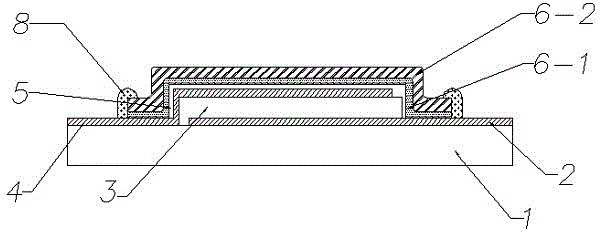
[0028] Such as image 3 As shown, a tape encapsulation structure of an organic light emitting diode has a front electrode 2 with ITO on the glass substrate 1, and includes an organic hole injection layer, an organic hole transport layer, an organic light emitting layer, an organic electron transport layer and The organic layer 3 of the organic electron injection layer, the metal aluminum rear electrode 4 and the protective layer 5 of the organic material are used for tape encapsulation of the organic light-emitting diode OLED of the bottom emission of the glass substrate, and the tape 6 used for the tape encapsulation of the OLED is a kind of A layer of self-adhesive layer 6-1 is coated under the aluminum foil belt 6-2 with good resistance to water vapor and oxygen passing through, and the adhesive tape 6 is rolled to make the self-adhesive layer 6 under a high-purity inert gas atmosphere. -1 is densely pasted on the OLED device, and the area of the adhesive tape 6 just cove...
PUM
| Property | Measurement | Unit |
|---|---|---|
| Thickness | aaaaa | aaaaa |
| Thickness | aaaaa | aaaaa |
| Thickness | aaaaa | aaaaa |
Abstract
Description
Claims
Application Information