Method for lowering influence on copper interconnection reliability from online WAT testing

A technology of copper interconnection and reliability, applied in semiconductor/solid-state device testing/measurement, electrical components, semiconductor/solid-state device manufacturing, etc., can solve the problems of thick oxide layer, dielectric material damage, dielectric The effect of reducing the reliability of copper interconnection, suppressing the formation of defects, and improving the interface bonding state

Active Publication Date: 2014-08-06
SHANGHAI HUALI MICROELECTRONICS CORP
View PDF5 Cites 15 Cited by
  • Summary
  • Abstract
  • Description
  • Claims
  • Application Information

AI Technical Summary

Problems solved by technology

During the conventional plasma repair process of the oxide layer, the dielectric material will be directly physically sputtered by high-energy ions and groups in the plasma, so it is more susceptible to damage and the dielectric constant increases
[0006] In summary, a single plasma surface treatment process cannot effectively repair the thick oxide layer on the metal surface, and it will inevitably cause certain damage to the dielectric material.

Method used


Image

  • Method for lowering influence on copper interconnection reliability from online WAT testing
  • Method for lowering influence on copper interconnection reliability from online WAT testing
  • Method for lowering influence on copper interconnection reliability from online WAT testing

Examples


Embodiment Construction
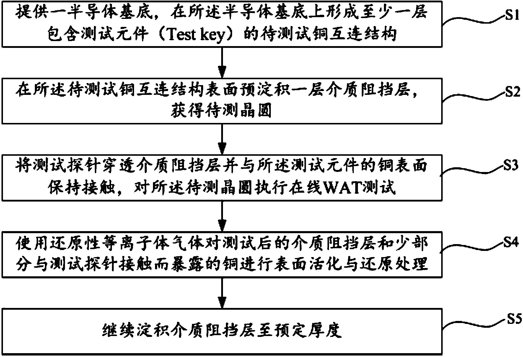
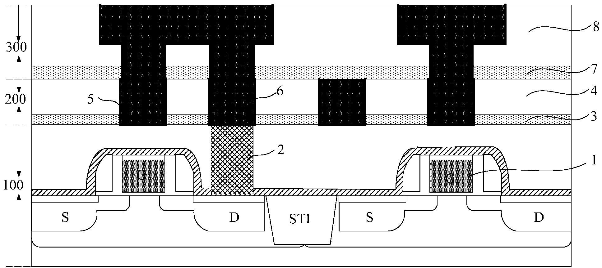
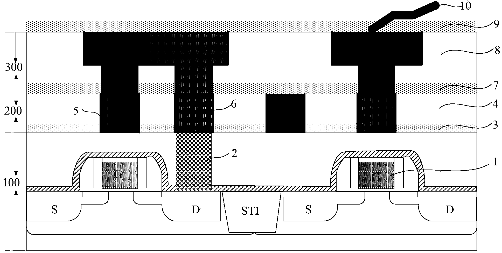
[0035] The core idea of ​​the invention is to disclose a method for reducing the influence of online wafer acceptance test on the reliability of copper interconnection. Among them, firstly, by pre-depositing a thinner dielectric barrier layer on the surface of the copper interconnection structure to be tested, the copper and dielectric material surfaces of the copper interconnection structure to be tested can be tested without affecting the execution of the online WAT test. During the process, it is well isolated and protected; then, by using reducing plasma gas to perform surface activation and reduction treatment on the pre-deposited dielectric barrier layer after the test and a small part of the exposed metal copper in contact with the test probe, it can be effectively removed. The oxides and residual impurities generated on the surface can improve the interface bonding state with the subsequent film; secondly, the dielectric material of the copper interconnection structure ...


PUM


Abstract

The invention provides a method for lowering the influence on the copper interconnection reliability from the online WAT testing. The method comprises the steps that at least one layer of to-be-tested copper interconnection structure comprising a testing component is formed on a semiconductor substrate; a dielectric barrier layer is deposited on the surface of the to-be-tested copper interconnection structure in advance, and a wafer to be tested is obtained; a testing probe penetrates through the dielectric barrier layer and keeps contact with the copper surface of the testing component, and online WAT testing is carried out on the wafer to be tested; surface activation and reduction treatment are carried out on the tested dielectric barrier layer and a small part of copper exposed after making contact with the testing probe through reducing plasma gas; the dielectric barrier layer continues to be deposited to be at the preset thickness. Through the method for combining the pre-deposited dielectric barrier layer serving as an isolation protection layer before the testing with the surface plasma activation and reduction treatment after the testing, defects in copper and dielectric materials are effectively restrained from being generated in the online WAT testing process, and the influence on the copper interconnection reliability from the online WAT testing is lowered significantly.

Description

technical field [0001] The invention relates to the field of semiconductor manufacturing, in particular to a method for reducing the influence of online WAT testing on the reliability of copper interconnection. Background technique [0002] Wafer Acceptance Test (WAT) refers to the electrical testing of the test structure on the wafer after the semiconductor wafer has completed all the manufacturing processes. Through the analysis of WAT data, problems in the semiconductor manufacturing process can be effectively monitored, which is helpful for the adjustment and optimization of the manufacturing process. With the gradual reduction of critical dimensions of semiconductors in integrated circuits, their integration level continues to increase, and the overall process technology is gradually becoming more complex. For example, the total number of process steps for 45nm technology logic products reaches more than 1000, and up to 12 metal interconnection layers need to be formed...

Claims


Application Information

Patent Timeline
Patent Type & Authority Applications(China)
IPC IPC(8): H01L21/768H01L21/66
CPCH01L22/12H01L22/14
Inventor 张磊姬峰胡友存陈玉文李磊
Owner SHANGHAI HUALI MICROELECTRONICS CORP
Why Eureka
Try Eureka