

Annealing and wool-making method for monocrystalline silicon wafer
A single-crystal silicon wafer, annealing technology, applied in chemical instruments and methods, crystal growth, post-processing details, etc., can solve the problems of uneven pyramid size and high reflectivity, and achieve good uniformity and suede reflectivity. low effect
- Summary
- Abstract
- Description
- Claims
- Application Information
AI Technical Summary
Problems solved by technology
Method used
Image

Examples
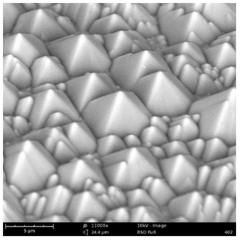
Embodiment 1
[0018] After the monocrystalline silicon chip is cleaned with a mixture of deionized water, 30% hydrogen peroxide aqueous solution and 30% ammonia aqueous solution in a volume ratio of 5:1 to 2:1, deionized water and The mass fraction is 30% hydrogen peroxide aqueous solution, and the mass fraction is 37% hydrochloric acid aqueous solution, and the volume ratio is 6~8:1~2:1 mixed solution cleaning; The monocrystalline silicon chip after cleaning is hydrofluoric acid, deionized The mixed solution of water and ethanol was rinsed for 1 minute, the volume fraction of hydrofluoric acid in the mixed solution was 8%, and the volume fraction of ethanol was 20%, and then dried with nitrogen; second, take out the silicon chip so that the surface of the silicon chip is stained with texturing liquid, and put it into the tube annealing furnace under N 2 Anneal at 400°C for 20 minutes in the atmosphere, and cool naturally to room temperature after annealing; then place the silicon wafer in ...
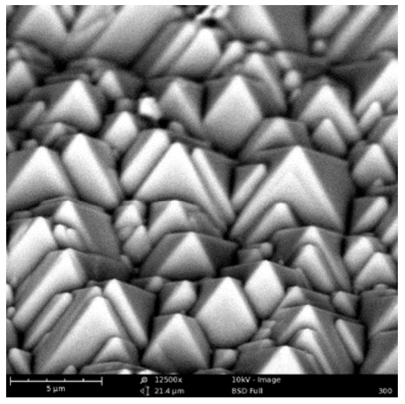
Embodiment 2
[0021] The annealing condition of the present embodiment is: at N 2 Annealing at 200° C. for 20 minutes under atmosphere, other steps are the same as in Example 1.
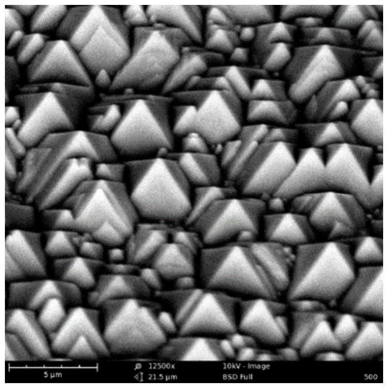
Embodiment 3
[0023] The annealing condition of the present embodiment is: at N 2 Annealing at 300° C. for 20 minutes under atmosphere, other steps are the same as in Example 1.
PUM
 Abstract
Description
Claims
Application Information