Electrostatic shielding effect transistor and design method thereof

A technology of electrostatic shielding and design method, applied in the direction of electric solid devices, circuits, electrical components, etc., can solve the impact resistance and high frequency radiation resistance to be improved, the secondary breakdown voltage resistance is poor, and the thermal stability is not good. and other problems, to achieve the effect of large power capacity and safe working area, high secondary breakdown voltage and good thermal stability

Active Publication Date: 2014-08-27
SHENZHEN SHENGYUAN SEMICON
View PDF3 Cites 8 Cited by
  • Summary
  • Abstract
  • Description
  • Claims
  • Application Information

AI Technical Summary

Problems solved by technology

As a new type of power device, transistors are becoming more and more popular. However, it is difficult for transistors to solve the problems of high frequency, high voltage, and high current; and it is difficult for them to have some advantages of MOS and BJT at the same time. Slow, poor secondary breakdown pressure resistance, poor thermal stability, impact resistance and high-frequency radiation resistance need to be improved

Method used


Image

  • Electrostatic shielding effect transistor and design method thereof
  • Electrostatic shielding effect transistor and design method thereof
  • Electrostatic shielding effect transistor and design method thereof

Examples


Embodiment Construction

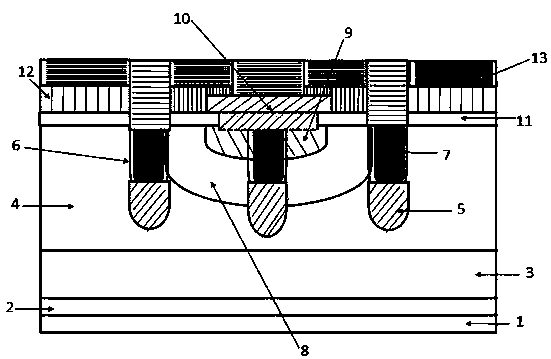
[0032] In order to make the object, technical solution and advantages of the present invention clearer, the present invention will be further described in detail below in conjunction with the accompanying drawings and embodiments. It should be understood that the specific embodiments described here are only used to explain the present invention, not to limit the present invention.

[0033] In the description of the present invention, it should be understood that the orientation or positional relationship indicated by the terms "upper", "lower", "front", "rear", "inner", "outer" etc. Orientation or positional relationship is only for the convenience of describing the present invention and simplifying the description, and does not indicate or imply that the referred device or element must have a specific orientation, be constructed and operated in a specific orientation, and thus should not be construed as a limitation of the present invention.

[0034] In the description of the...


PUM


Abstract

The invention discloses an electrostatic shielding effect transistor. The electrostatic shielding effect transistor comprise a collector, groove-type grids, a base region, an oxidization layer, a polycrystalline silicon layer and emitters. The collector comprises a leading-out end, an N+ substrate, an N+ conductive material layer and an N- conductive material layer. The groove-type grids are arranged on the N- conductive material layer, B ions of certain concentration are injected into the bottom of a groove to serve as P+ regions, and the base region injected with the B ions is arranged between the grids. The oxidization layer is arranged on the grids and the base region, the emitters are formed on the base region and the oxidization layer, the polycrystalline silicon layer is deposited on the oxidization layer and the polycrystalline silicon layer forms an emitting region below the emitters after high-temperature diffusion. The electrostatic shielding effect transistor is provided with the emitters and the base region which are super shallow in junction and small in size, and therefore, the emitter current crowding effect and the base region flow extruding effect of the device can be greatly improved. Due to the super small junction depth of the structure and the base region of the device, the hole extraction speed is increased and the high frequency property of the device is improved.

Description

technical field [0001] The invention belongs to the technical field of semiconductor components and relates to an electrostatic shielding effect transistor and a design method thereof. Background technique [0002] Power devices are the core devices of the modern power electronics industry. Semiconductor new energy technology and national energy saving and consumption reduction policies are inseparable from the support of power devices, such as MOSFETs and IGBTs developed based on MOSFETs. As a new type of power device, transistors are becoming more and more popular. However, it is difficult for transistors to solve the problems of high frequency, high voltage, and high current; and it is difficult for them to have some advantages of MOS and BJT at the same time. Slow, poor secondary breakdown pressure resistance, poor thermal stability, impact resistance and high-frequency radiation resistance need to be improved. [0003] Therefore, it is necessary to conduct research to ...

Claims


Application Information

Patent Timeline
Patent Type & Authority Applications(China)
IPC IPC(8): H01L29/78H01L23/60H01L29/06H01L21/265
CPCH01L29/7393H01L29/0834H01L29/1004H01L29/66325
Inventor 张雷
Owner SHENZHEN SHENGYUAN SEMICON
Why Eureka
Try Eureka