Organic electroluminescent device and preparation method
An electroluminescent device and electroluminescent technology, applied in the direction of electric solid device, semiconductor/solid state device manufacturing, electrical components, etc., can solve the problems of refractive index difference, light loss, low light output performance, etc., to improve light output efficiency, avoid The effect of the phenomenon of total reflection
- Summary
- Abstract
- Description
- Claims
- Application Information
AI Technical Summary
Problems solved by technology
Method used
Image
Examples
Embodiment 1
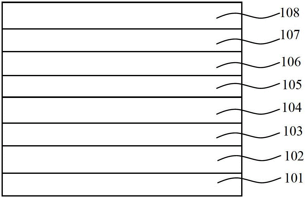
[0081] A method for preparing an organic electroluminescent device, comprising the following steps:
[0082] (1) After rinsing the N-LASF44 glass with distilled water and ethanol, soak it in isopropanol for one night to obtain a clean glass substrate;
[0083] (2) In the high vacuum coating system (Shenyang Scientific Instrument Development Center Co., Ltd.), the pressure is 5×10 -4 Under the condition of Pa, thermal resistance vapor deposition of Ta on one side of a clean glass substrate at a deposition rate of 4nm / s 2 o 5 Prepare a light extraction layer with a thickness of 150nm. On the other side of the glass substrate, thermally resistively evaporate a mixture of Au:CuO to prepare an anode with a thickness of 10nm. The Au:CuO mixture is formed by doping CuO into Au at a mass fraction of 30%. mixture;
[0084] (3) At a pressure of 5×10 -4 Under the condition of Pa, the hole injection layer, the hole transport layer, the light emitting layer and the electron transport l...
Embodiment 2
[0092] A method for preparing an organic electroluminescent device, comprising the following steps:
[0093] (1) After rinsing the N-LAF36 glass with distilled water and ethanol, soak it in isopropanol for one night to obtain a clean glass substrate;
[0094] (2) In the high vacuum coating system (Shenyang Scientific Instrument Development Center Co., Ltd.), the pressure is 2×10 -3 Under the condition of Pa, thermal resistance evaporation of Nb on one side of a clean glass substrate with an evaporation rate of 1nm / s 2 o 5 Prepare a light extraction layer with a thickness of 200nm, and thermally resistively evaporate Pt:Ag on the other side of the glass substrate 2 O mixture to prepare anode with a thickness of 5nm, where Pt:Ag 2 O mixture for the Ag 2 A mixture formed by doping O into Pt according to 50% mass fraction;
[0095] (3) At a pressure of 2×10 -3 Under the condition of Pa, the hole injection layer, the hole transport layer, the light emitting layer and the elec...
Embodiment 3
[0099] A method for preparing an organic electroluminescent device, comprising the following steps:
[0100] (1) After rinsing the N-LASF41 glass with distilled water and ethanol, soak it in isopropanol for one night to obtain a clean glass substrate;
[0101] (2) In the high vacuum coating system (Shenyang Scientific Instrument Development Center Co., Ltd.), the pressure is 5×10 -5 Under the condition of Pa, thermal resistance vapor deposition of VO on one side of a clean glass substrate at a deposition rate of 10nm / s 2 Prepare a light extraction layer with a thickness of 50nm, and thermally resistively evaporate Ag:Cu on the other side of the glass substrate 2 O mixture to prepare anode with a thickness of 20nm, where Ag:Cu 2 O mixture is the Cu 2 A mixture formed by doping O into Ag according to the mass fraction of 20%;
[0102] (3) At a pressure of 5×10 -5 Under the condition of Pa, the hole injection layer, the hole transport layer, the light emitting layer and the ...
PUM
| Property | Measurement | Unit |
|---|---|---|
| Thickness | aaaaa | aaaaa |
| Thickness | aaaaa | aaaaa |
| Thickness | aaaaa | aaaaa |
Abstract
Description
Claims
Application Information

