

Array substrate of display device and manufacturing method of array substrate of display device
A technology for array substrates and display devices, applied in semiconductor/solid-state device manufacturing, electric solid-state devices, semiconductor devices, etc., can solve the problems of high power consumption, small redundancy, and low compatibility, and achieve simplified manufacturing process steps, High design redundancy and the effect of reducing parasitic capacitance
- Summary
- Abstract
- Description
- Claims
- Application Information
AI Technical Summary
Problems solved by technology
Method used
Image

Examples
Embodiment Construction
[0051] The present invention will be further described below based on specific embodiments and drawings, but it is not a limitation of the present invention.
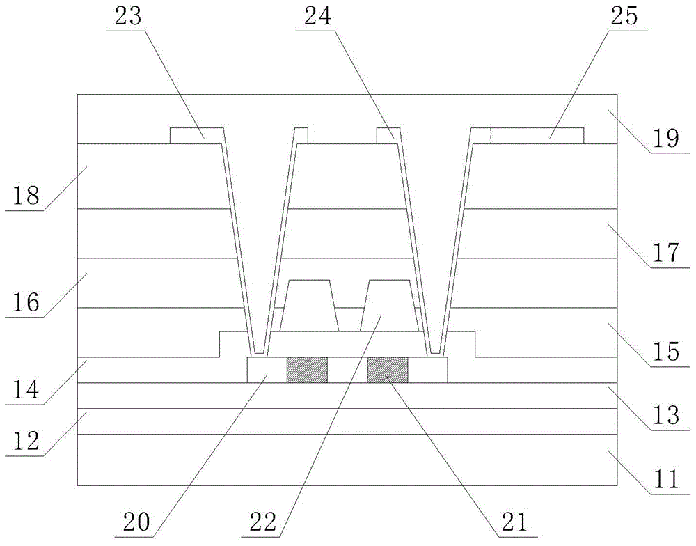
[0052] figure 1 Is a schematic diagram of an embodiment of the array substrate of the display device of the present invention; figure 1 As shown, an array substrate of a display device includes a substrate structure composed of a glass substrate (glass) 11, a bottom silicon nitride layer (BL-SiN) 12, and a bottom silicon oxide layer (BL-SiO) 13, and the bottom The silicon nitride layer 12 covers the upper surface of the glass substrate 11, and the bottom silicon oxide layer 13 covers the upper surface of the bottom silicon nitride layer 12.
[0053] Further, the upper surface of the substrate structure (ie the bottom silicon oxide layer) is also provided with active / drain regions 20 (such as P-type S / D), and between adjacent source / drain regions 20 is also provided The channel region 21, the aforementioned source / drain regio...
PUM
 Abstract
Description
Claims
Application Information