Organic light emission diode and preparation method thereof

An electroluminescent device and luminescent technology, applied in the field of electric light sources, can solve the problems of poor OLED stability, short service life, and increased bandgap width, and achieve the effects of high qualified rate of finished products, reduced production costs, and improved production efficiency

Inactive Publication Date: 2014-09-10
OCEANS KING LIGHTING SCI&TECH CO LTD +2
View PDF4 Cites 0 Cited by
  • Summary
  • Abstract
  • Description
  • Claims
  • Application Information

AI Technical Summary

Problems solved by technology

[0005] However, in practical applications, it is found that the organic electroluminescent materials used in the organic functional layers of OLEDs are particularly sensitive to the intrusion of oxygen and water vapor, resulting in poor stability and short service life of OLEDs, which affects the popularization and application of OLEDs.
This is because oxygen is a triplet quencher, which significantly reduces the quantum efficiency of luminescence; on the other hand, the oxidation of oxygen to the luminescent layer will generate carbonyl compounds, which

Method used


Image

  • Organic light emission diode and preparation method thereof
  • Organic light emission diode and preparation method thereof
  • Organic light emission diode and preparation method thereof

Examples


preparation example Construction

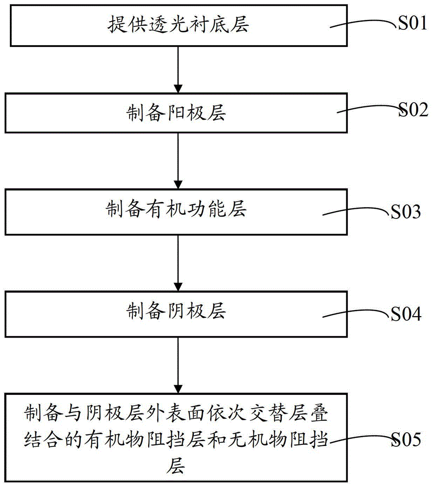
[0050] Correspondingly, the embodiment of the present invention also provides a preparation method of the above-mentioned organic electroluminescence device. The process flow chart of the method is as image 3 Therefore, see also Figure 1~2 , the method includes the following steps:

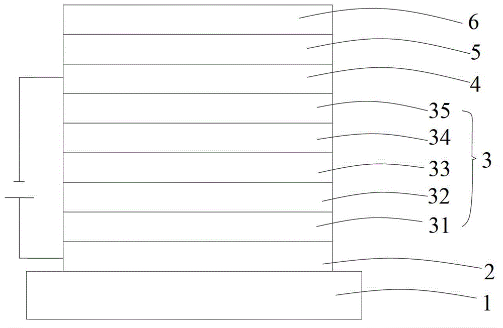
[0051] S01. Provide a light-transmitting substrate layer 1;

[0052] S02. Prepare the anode layer 2: plate the anode layer 2 on the surface of the transparent substrate layer 1 in step S01;

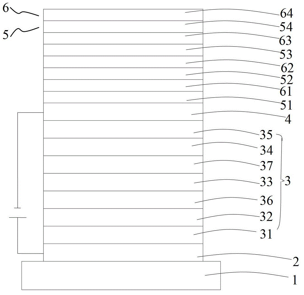
[0053] S03. Preparation of organic functional layer 3: In step S02, the surface opposite to the surface of the anode layer 2 prepared with the light-transmitting substrate layer 1 is sequentially plated with a hole injection layer 31, a hole transport layer 32, a light-emitting layer 33, and an electron transport layer 34. , the electron injection layer 35, forming the organic functional layer 3;

[0054] S04. Prepare the cathode layer 4: plate the cathode layer 4 on the outer surface of the organic fun...

Embodiment 1

[0077] An organic electroluminescence device, its structure is: glass substrate / ITO / MoO 3 :NPB / TCTA / TPBI:Ir(ppy) 3 / Bphen / CsN 3 :Bphen / Al / (TPD:Bphen / Sb 2 Se 3 :Si 3 N 4 :AlB 2 ) 6 .

[0078] The preparation method of the organic electroluminescence device comprises the following steps:

[0079] a) Pre-treatment of ITO glass substrate: cleaning with acetone→cleaning with ethanol→cleaning with deionized water→cleaning with ethanol, all of them are cleaned with an ultrasonic cleaner, and the single washing is cleaned for 5 minutes, then blown dry with nitrogen, and dried in an oven for later use; The cleaned ITO glass also needs surface activation treatment to increase the oxygen content of the conductive surface layer and improve the work function of the conductive layer surface; the thickness of ITO is 100nm;

[0080] b) Preparation of the organic functional layer: sequentially coat the outer surface of the ITO layer in step a) with a hole injection layer, a hole trans...

Embodiment 2

[0091] An organic electroluminescence device, its structure is: glass substrate / ITO / MoO 3 :NPB / TCTA / TPBI:Ir(ppy) 3 / Bphen / CsN 3 :Bphen / Al / (BCP:NPB / MoSe 2 :AlN:LaB 6 ) 6 .

[0092] The preparation method of the organic electroluminescence device comprises the following steps:

[0093] a), b), c) are the same as in Example 1;

[0094] d) Fabrication of the organic barrier layer: the organic barrier layer is made of NPB as the hole transport material and BCP doped co-evaporation as the electron transport material, wherein the hole transport material accounts for 50% of the total molar percentage of the organic barrier layer material, and vacuum Prepared by evaporation, vacuum degree 5×10 -5 Pa, evaporation rate Thickness 250nm;

[0095] e) Preparation of inorganic barrier layer: the inorganic barrier layer is made of selenide, nitride and boride doped magnetron sputtering, and the selenide is MoSe 2 , the nitride is AlN, the boride is LaB 6 , where MoSe 2 Accounting ...


PUM

PropertyMeasurementUnit
Thicknessaaaaaaaaaa
Thicknessaaaaaaaaaa
Thicknessaaaaaaaaaa

Abstract

The invention discloses an organic light emission diode (OLED) and a preparation method thereof. The organic light emission diode comprises a transparent substrate layer, an anode layer, an organic functional layer, a cathode layer, an organic barrier layer and an inorganic barrier layer, wherein the transparent substrate layer, the anode layer, the organic functional layer, and the cathode layer are successively laminated and combined and the organic barrier layer and the inorganic barrier layer are successively and alternately laminated and combined at the outer surface of the cathode layer. Materials used by the inorganic barrier layer include selenides, nitrides, and borides, wherein the components are doped mutually; the selenides account for 10% to 30%, by weight, of the total weight of the inorganic barrier layer materials; and the borides account for 10% to 30%, by weight, of the total weight of the inorganic barrier layer materials. According to the invention, corrosion of active materials like water and oxygen and the like on the organic light emission diode can be effectively reduced, thereby obviously improving the stable performance of the OLED and prolonging the service life of the OLED. Besides, the preparation method has advantages of simple process, easily-controlled condition, and easily-large area preparation.

Description

technical field [0001] The invention belongs to the technical field of electric light sources, and in particular relates to an organic electroluminescent device and a preparation method thereof. Background technique [0002] Organic Light Emission Diode (hereinafter referred to as OLED) is a current-mode semiconductor light-emitting device based on organic materials. Its typical structure is to make a layer of tens of nanometers thick organic light-emitting material on the ITO glass as the light-emitting layer, and there is a metal electrode with a low work function above the light-emitting layer. [0003] The principle of OLED light emission is based on the action of an external electric field, electrons are injected from the cathode to the lowest unoccupied molecular orbital (LUMO) of organic matter, and holes are injected from the anode to the highest occupied orbital (HOMO) of organic matter. Electrons and holes meet, recombine, and form excitons in the light-emitting l...

Claims


Application Information

Patent Timeline
IPC IPC(8): H01L51/52H01L51/54H01L51/56
CPCH10K50/8445H10K50/844
Inventor 周明杰钟铁涛张娟娟王平
Owner OCEANS KING LIGHTING SCI&TECH CO LTD
Why Eureka
Try Eureka