A kind of metal oxide TFT device and manufacturing method

A manufacturing method and oxide technology, applied in semiconductor/solid-state device manufacturing, electric solid-state devices, semiconductor devices, etc., can solve problems such as process and complexity that are prone to parasitic capacitance, avoid adverse effects, improve selectivity, and improve Quasi-precise effect

Inactive Publication Date: 2017-12-12
SHENZHEN ROYOLE TECH CO LTD
View PDF6 Cites 2 Cited by
  • Summary
  • Abstract
  • Description
  • Claims
  • Application Information

AI Technical Summary

Problems solved by technology

[0006] The purpose of the present invention is to provide a method for manufacturing a metal oxide TFT device, which aims to solve the problem that the traditional method is prone to produce parasitic capacitance and the process is complex

Method used


Image

  • A kind of metal oxide TFT device and manufacturing method
  • A kind of metal oxide TFT device and manufacturing method
  • A kind of metal oxide TFT device and manufacturing method

Examples


Embodiment 2

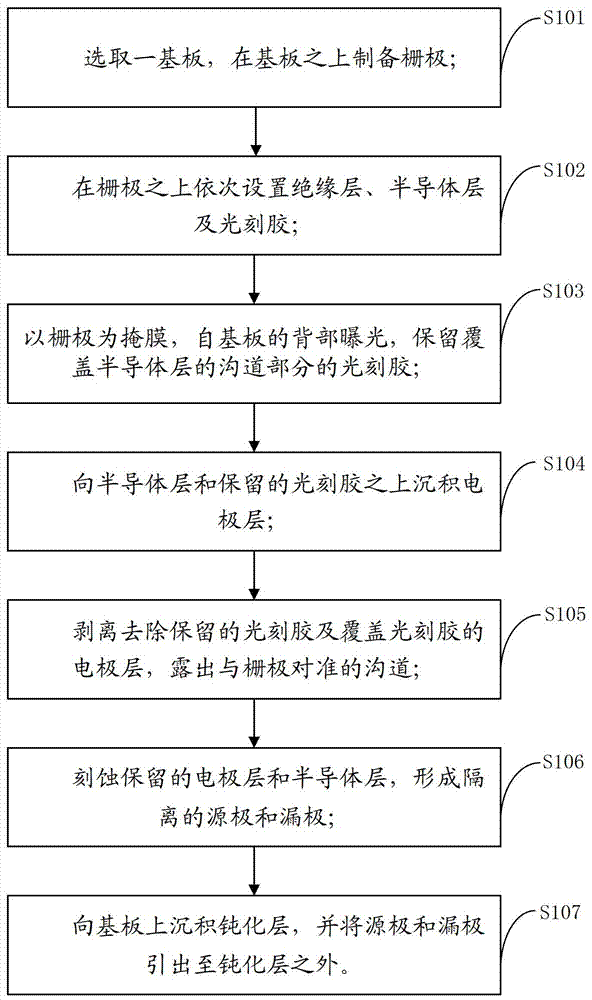
[0076] Figure 5 It shows the flow chart of the manufacturing method of the metal oxide TFT pixel circuit provided by the second embodiment of the present invention, Figure 6-1~6-11 A schematic structural diagram corresponding to the manufacturing method is shown, and for convenience of description, only parts related to this embodiment are shown.

[0077] Such as Figure 5 , the method includes the following steps:

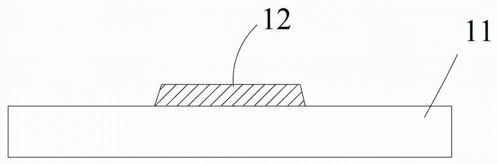
[0078] In step S201, a substrate 21 is selected, and a gate 221, a gate lead 222 and a storage capacitor electrode 223 are prepared on the substrate 21; Figure 6-1 .

[0079] In this step, a buffer layer may also be provided on the substrate 21 first.

[0080] In step S202, an insulating layer 23, a semiconductor layer 24 and a photoresist 25 are sequentially provided on the gate 221, the gate lead 222 and the storage capacitor electrode 223; Figure 6-2 , 6-3 , 6-4.

[0081] In this step, an insulating layer 23 is first deposited on the substrate 21 and...


PUM


Abstract

The present invention is applicable to the technical field of electronic devices, and provides a method for manufacturing a metal oxide TFT device, comprising selecting a substrate and preparing a gate on the substrate; sequentially disposing an insulating layer, a semiconductor layer and a photoresist on the gate; The gate is a mask, which is exposed from the back of the substrate, and the photoresist covering the channel part of the semiconductor layer is retained; the electrode layer is deposited on the semiconductor layer and the photoresist; the photoresist and the electrode layer covering the photoresist are peeled off to expose channel; etch the electrode layer and semiconductor layer to form an isolated source and drain; deposit a passivation layer to lead out the source and drain. In the present invention, the gate is used as a mask to realize self-alignment through back exposure and photoresist stripping, the process is simple and the alignment accuracy is high, the parasitic capacitance is weakened, the performance of the device is improved, and no etching barrier layer is required. The process is simplified, the bad influence of the etching barrier layer on the semiconductor channel is avoided, and the alignment of the mask plate is no longer a key alignment requirement, thereby reducing the manufacturing difficulty.

Description

technical field [0001] The invention belongs to the technical field of electronic devices, in particular to a metal oxide TFT device and a manufacturing method thereof. Background technique [0002] Metal oxide thin film transistor (TFT) is a basic circuit component device that can be widely used in various electronic systems, and it has many advantages, such as high electron mobility, low temperature manufacturing process, high stability, high transparency, etc. . Such as figure 1 As shown, in the traditional TFT manufacturing process, the alignment of the gate (Gate) 101, the source (Source) 102, and the drain (Drain) 103 of the TFT device is done manually or mechanically by using two different mask plates. achieved by optical alignment. Due to the limitation of the accuracy of the alignment equipment and other factors, this method will cause a certain overlap between the source 102, the drain 103 and the gate 101, resulting in a large gate-source parasitic capacitance ...

Claims


Application Information

Patent Timeline
Patent Type & Authority Patents(China)
IPC IPC(8): H01L21/28H01L29/786G02F1/1362
CPCH01L27/1225H01L21/0272H01L21/467H01L21/47635H01L27/124H01L27/1255H01L27/1259H01L27/1288H01L29/41733H01L29/41775H01L29/42356H01L29/66969H01L29/7869
Inventor 魏鹏余晓军刘自鸿
Owner SHENZHEN ROYOLE TECH CO LTD
Why Eureka
Try Eureka