NLDMOS device and manufacturing method thereof

A device, N-type technology, used in semiconductor/solid-state device manufacturing, semiconductor devices, electrical components, etc., can solve the problems of low on-resistance, reduce device breakdown voltage, increase process complexity and cost, and reduce conduction. The effect of on-resistance, increasing on-current, and avoiding breakdown voltage drop

Active Publication Date: 2014-09-24
SHANGHAI HUAHONG GRACE SEMICON MFG CORP
View PDF3 Cites 4 Cited by
  • Summary
  • Abstract
  • Description
  • Claims
  • Application Information

AI Technical Summary

Problems solved by technology

It is usually necessary to add an additional N-type implant in the drift region of the device to make the device have a lower on-resistance, and this method will reduce the breakdown voltage of the device and increase process complexity and cost

Method used


Image

  • NLDMOS device and manufacturing method thereof
  • NLDMOS device and manufacturing method thereof
  • NLDMOS device and manufacturing method thereof

Examples


Embodiment Construction

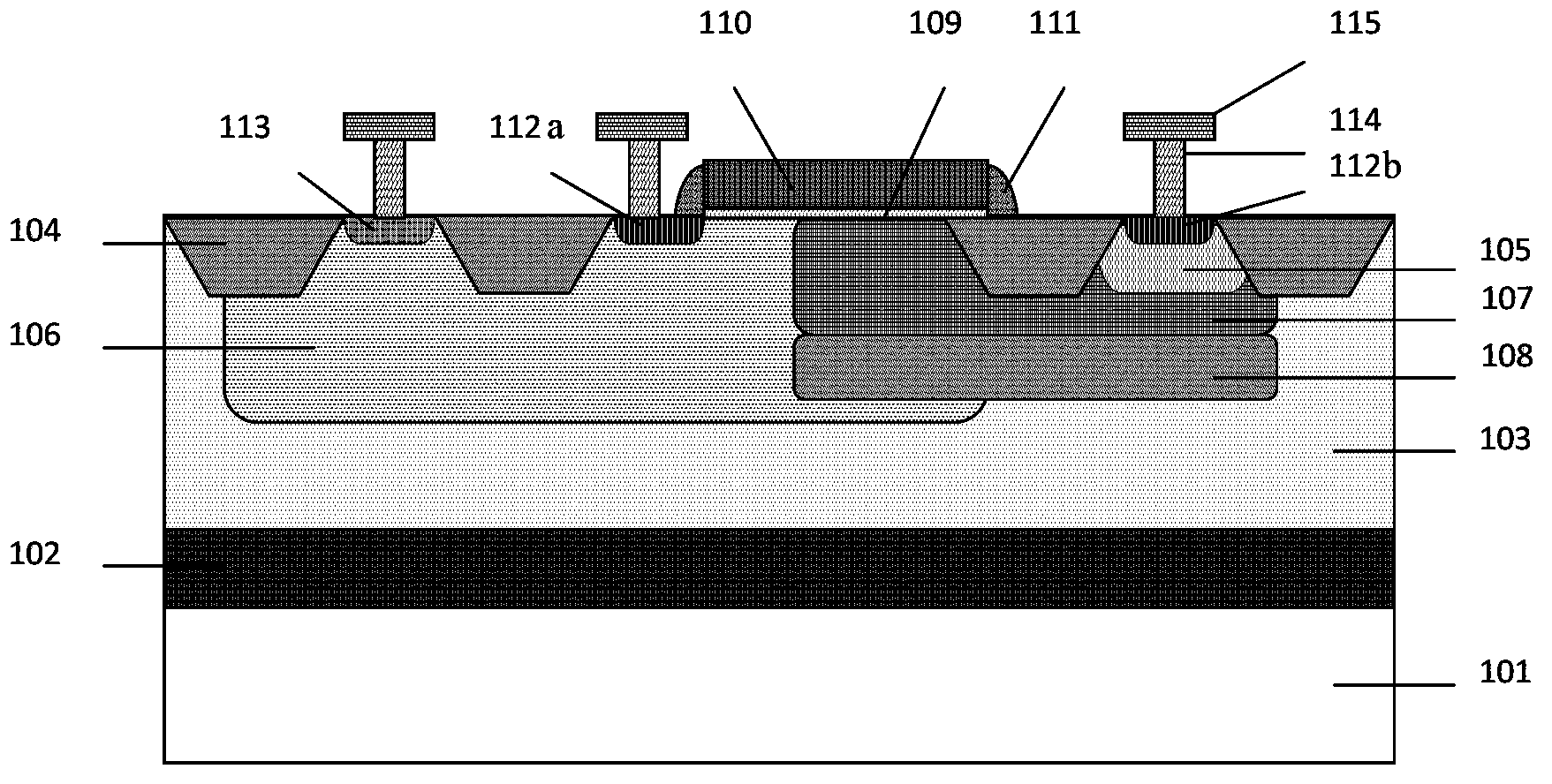
[0032] like figure 1 Shown is a schematic structural diagram of an N-type NLDMOS device in an embodiment of the present invention; the NLDMOS device in an embodiment of the present invention includes:

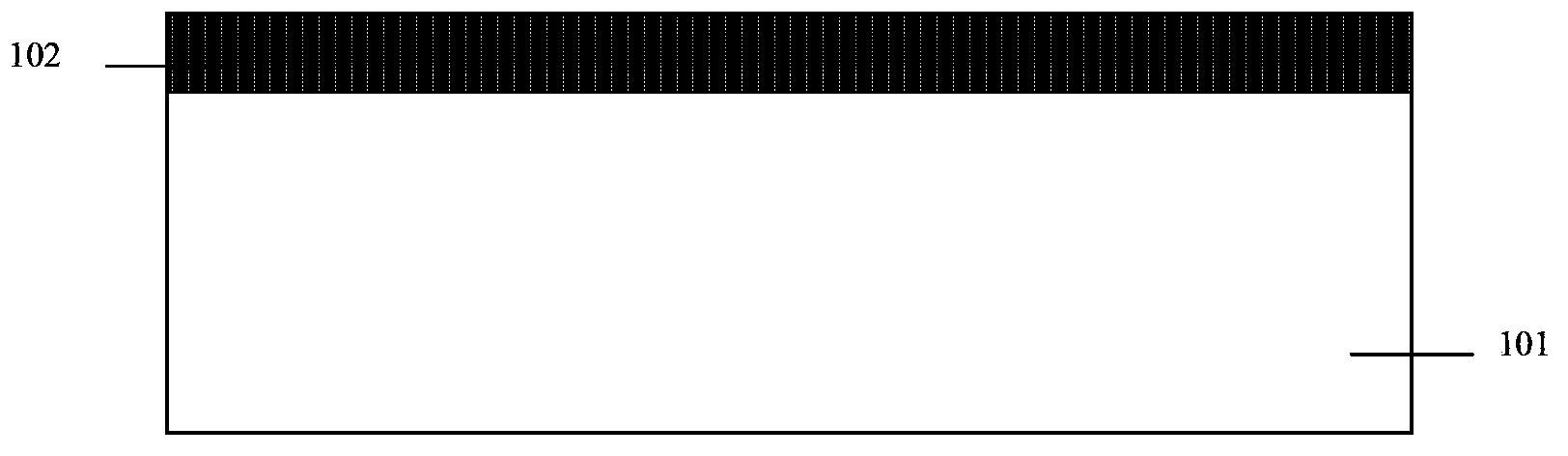
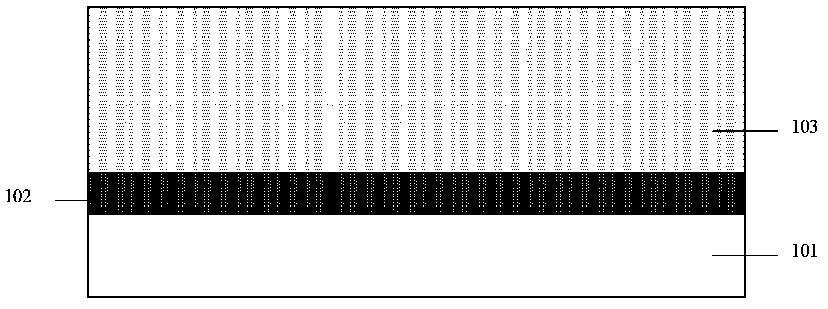
[0033] An N-type epitaxial layer 103 is formed on the semiconductor substrate, and a shallow trench isolation 104 structure is formed on the N-type epitaxial layer 103 . Preferably, the semiconductor substrate is an N+ doped silicon substrate 101, and the resistivity of the silicon substrate 101 is 0.007Ω·cm~0.013Ω·cm; N+ Buried layer 102 ; the N-type epitaxial layer 103 is formed on the N+ buried layer 102 .

[0034] The P well 106 is formed in the N-type epitaxial layer 103 , and the doping concentration of the P well 106 is greater than the doping concentration of the N-type epitaxial layer 103 .

[0035] The N well 105 is formed in the N-type epitaxial layer 103, and the shallow trench isolation 104 is isolated between the N well 105 and the P well 106, and the shallow tr...


PUM


Abstract

The invention discloses an NLDMOS device. A drift region is composed of a first N-type ion injection region which is formed in an N-type epitaxial layer, a first P-type ion injection region which is arranged on the bottom part of the first N-type ion injection region, and an N-type epitaxial layer. The first N-type ion injection region can greatly increase conduction current and reduce conduction resistance; and longitudinal exhausting can be performed on the first N-type ion injection region from the bottom part by the first P-type ion injection region so that electric field distribution in the drift region can be changed, a device surface electric field can be reduced, voltage-withstanding performance of the device can be enhanced and reduction of breakdown voltage of the device can be avoided when conduction current increases. The invention also discloses a manufacturing method for the NLDMOS device. The NLDMOS device is great in compatibility with an existing BCD technology platform, stable in technology and relatively low in cost.

Description

technical field [0001] The invention relates to the field of manufacturing semiconductor integrated circuits, in particular to an NLDMOS (N-type lateral double-diffused metal-oxide-semiconductor field-effect transistor) device, and the invention also relates to a method for manufacturing the NLDMOS device. Background technique [0002] DMOS (Double Diffused Metal Oxide Semiconductor Field Effect Transistor) is currently widely used in power management circuits due to its high voltage resistance, high current drive capability and extremely low power consumption. In LDMOS (Lateral Double Diffused Metal Oxide Semiconductor Field Effect Transistor) devices, on-resistance is an important indicator. In the BCD process (the process of making bipolar transistors, CMOS and DMOS devices on the same chip), although DMOS and CMOS (complementary metal oxide semiconductor) are integrated in the same chip, due to the high withstand voltage and Requirements for low on-resistance. Under the...

Claims


Application Information

Patent Timeline
Patent Type & Authority Applications(China)
IPC IPC(8): H01L29/78H01L29/06H01L21/336
CPCH01L29/063H01L29/66568H01L29/7816
Inventor 石晶韩峰陈雄斌刘冬华
Owner SHANGHAI HUAHONG GRACE SEMICON MFG CORP
Why Eureka
Try Eureka