Method for producing MOS transistor

A MOS transistor and semiconductor technology, which is applied in the manufacture of transistors, semiconductor devices, semiconductor/solid-state devices, etc., can solve the problems of obvious hot carrier injection effect, poor reliability, unstable negative bias temperature, etc. Small hot carrier effect, reducing instability, reducing the effect of electron-hole pairs

Inactive Publication Date: 2014-10-01
SEMICON MFG INT (SHANGHAI) CORP
View PDF3 Cites 7 Cited by
  • Summary
  • Abstract
  • Description
  • Claims
  • Application Information

AI Technical Summary

Problems solved by technology

[0006] The problem solved by the invention is that the negative bias temperature instability effect and hot carrier injection effect are obvious in the MOS transistor formed in the prior art, and the reliability is not good

Method used


Image

  • Method for producing MOS transistor
  • Method for producing MOS transistor
  • Method for producing MOS transistor

Examples


Embodiment Construction

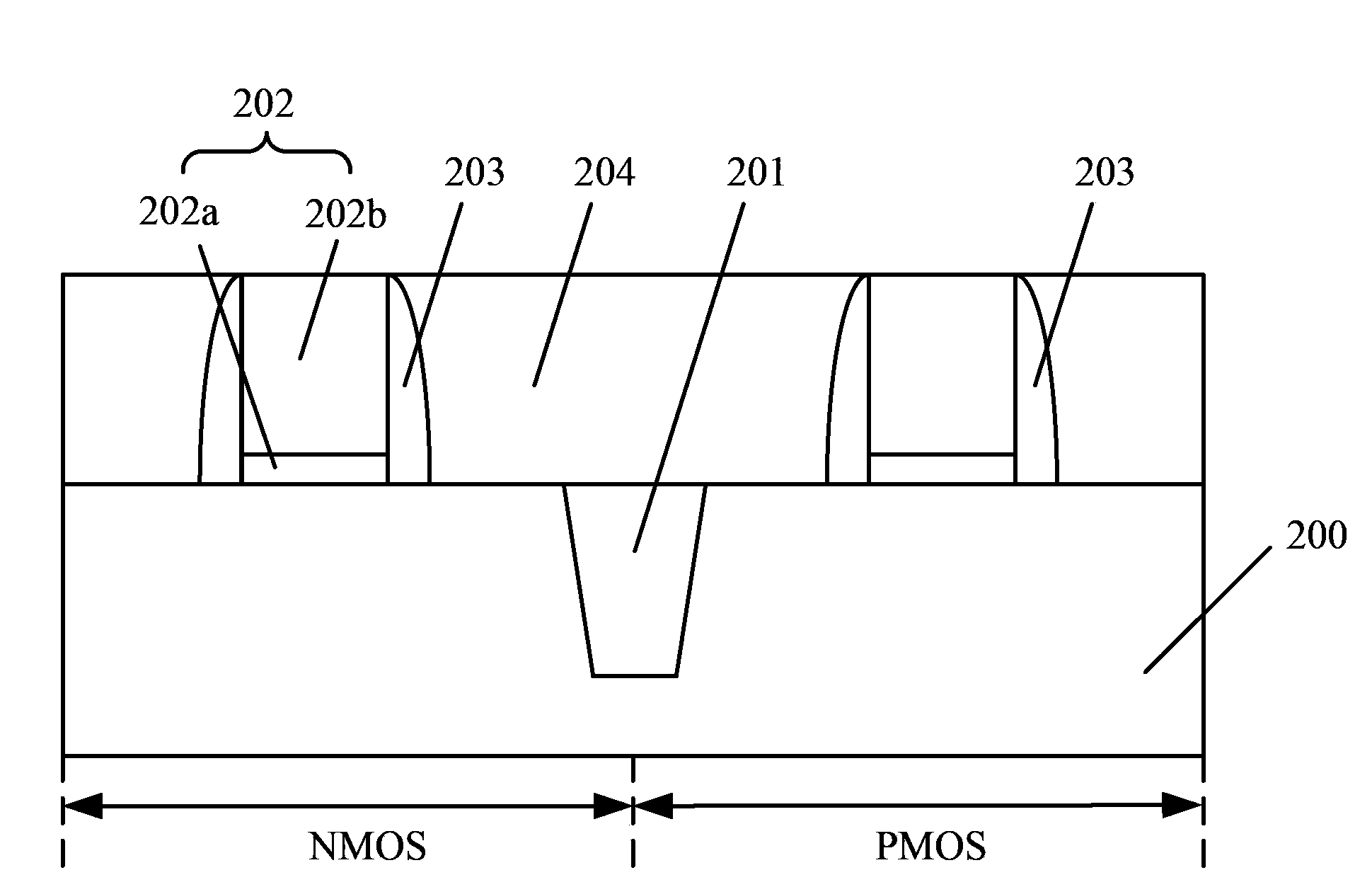
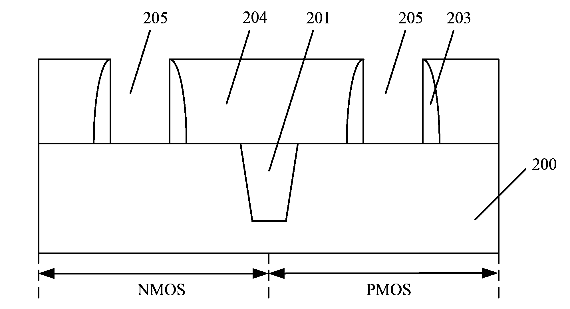
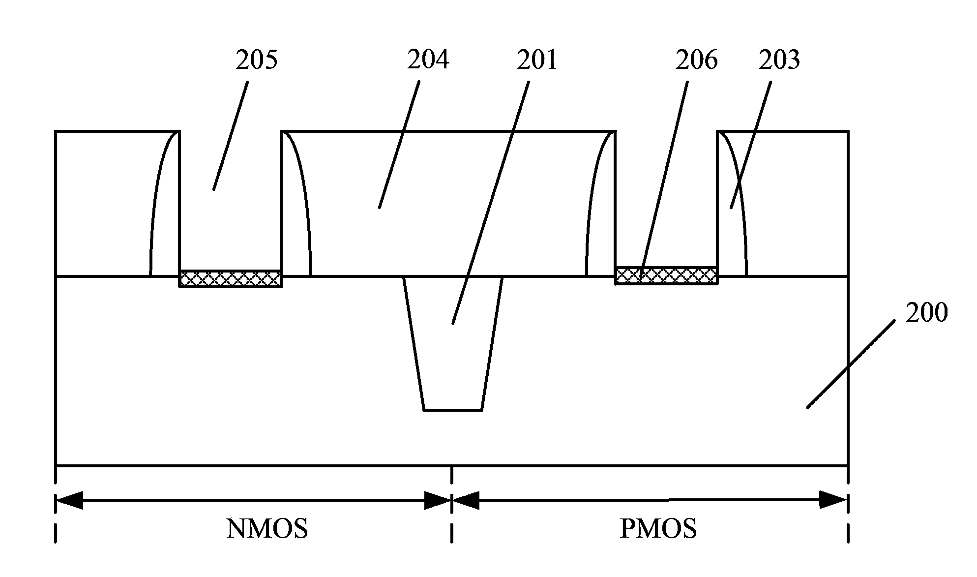
[0030] It can be seen from the background art that the negative bias temperature instability effect and the hot carrier injection effect are obvious in the MOS transistor formed in the prior art, and the reliability is not good.

[0031] The inventors of the present invention have found that the temperature instability effect of negative bias voltage is mainly caused by the change of trapped charge and oxide layer charge at the interface between silicon and gate dielectric layer through the research on the effect of negative bias temperature instability in MOS transistors. . There are some dangling bonds of silicon in the interface between the silicon of the gate and the gate dielectric layer. It is generally believed that these dangling bonds combine with hydrogen to form silicon-hydrogen (Si-H) bonds, which is called hydrogen passivation. However, a high electric field is formed on the gate during the operation of the transistor, and the silicon-hydrogen bond is easily broke...


PUM


Abstract

A method for producing an MOS transistor comprises the steps that a semiconductor substrate is provided, the surface of the semiconductor substrate is provided with dummy grids, side walls and dielectric layers, wherein the side walls are located at the two sides of the dummy grids, the semiconductor substrate and the side walls are covered with the dielectric layers, and the top surfaces of the dielectric layers are flush with the top surfaces of the dummy grids; the dummy grids are removed, so that openings are formed and parts of the surface of the semiconductor substrate are exposed through the openings; fluoridation is conducted on the parts, exposed through the openings, of the surface of the semiconductor substrate through a fluorine-containing solution, so that fluorine-containing surfaces are formed; interface layers are formed on the fluorine-containing surfaces; grid dielectric layers are formed on the interface layers and grid electrodes are formed on the grid dielectric layers. According to the method for producing the MOS transistor, the negative bias temperature instability effect and the hot carrier injection effect are lowered and the reliability of the MOS transistor is high.

Description

technical field [0001] The invention relates to the technical field of semiconductors, in particular to a method for forming a MOS transistor. Background technique [0002] With the continuous development of semiconductor technology, the feature size of MOS transistors is continuously reduced, and the thickness of the gate dielectric layer of MOS transistors is also becoming thinner and thinner according to the principle of proportional reduction. The silicon oxide layer has reached its physical limit as a gate dielectric layer. Using a high-K gate dielectric layer to replace the silicon oxide gate dielectric layer can greatly increase its physical thickness while keeping the equivalent oxide thickness (EOT) constant, thereby reducing The gate leakage current is reduced. However, since the high-K gate dielectric layer is mostly metal ion oxide, and there is no fixed atomic coordination, the stability of the bond between it and the silicon substrate is compared with the stab...

Claims


Application Information

Patent Timeline
Patent Type & Authority Applications(China)
IPC IPC(8): H01L21/336
CPCH01L29/66568H01L29/42356
Inventor 谢欣云
Owner SEMICON MFG INT (SHANGHAI) CORP
Why Eureka
Try Eureka