Copper bump package interconnection structure and method filled with double-layer underfill glue

An interconnection structure and double-bottom technology, applied in the direction of electrical components, electrical solid devices, circuits, etc., can solve the problems of unsatisfactory reliability of copper bumps and the inability to reduce stress at the chip end, and improve electrical connection characteristics and effects of mechanical stability, stress reduction, and high electrical connection characteristics

Active Publication Date: 2017-02-01
SHANGHAI INST OF MICROSYSTEM & INFORMATION TECH CHINESE ACAD OF SCI
View PDF5 Cites 0 Cited by
  • Summary
  • Abstract
  • Description
  • Claims
  • Application Information

AI Technical Summary

Problems solved by technology

At present, the industry still uses the traditional method for underfill filling, which cannot effectively reduce the stress on the chip end, resulting in unsatisfactory reliability of copper bumps.

Method used


Image

  • Copper bump package interconnection structure and method filled with double-layer underfill glue
  • Copper bump package interconnection structure and method filled with double-layer underfill glue
  • Copper bump package interconnection structure and method filled with double-layer underfill glue

Examples


Embodiment Construction

[0051] In order to fully demonstrate the advantages and positive effects of the present invention, the substantive features and remarkable progress of the present invention will be further described below in conjunction with the accompanying drawings and embodiments.

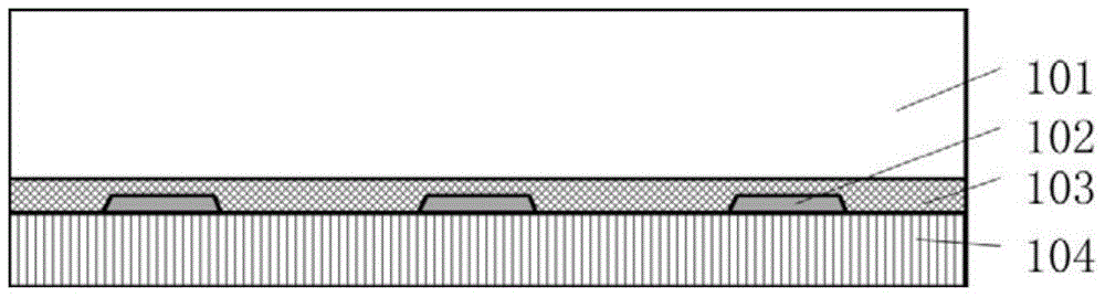
[0052] figure 1 On the active surface of the chip, a layer of thicker photoresist 104 is coated, wherein the pitch of the bumps is 120 μm, the diameter of the UBM opening is about 60 μm, and the thickness of the photoresist is about 30 μm.

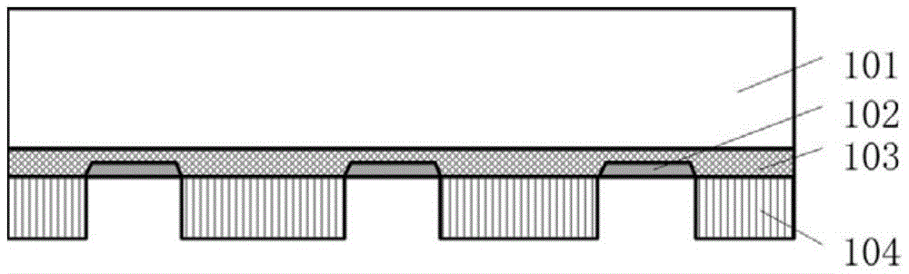
[0053] figure 2 It is exposed at the position corresponding to the UBM, and the UBM is exposed at the corresponding position after development.

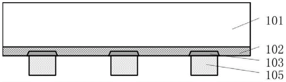
[0054] image 3 It is a schematic diagram of the copper bump shape formed by sputtering a seed layer at the copper bump position, followed by electroplating and glue removal. The copper bumps are 60 μm in diameter and 30 μm high.

[0055] Figure 4 After the copper bumps are plated, the first layer of underfill glue is spin-...


PUM


Abstract

The invention relates to a packaging and interconnecting structure and method for copper protruded points filled up with double layers of underfill. The packing and interconnecting structure is characterized in that the chip end is filled up with the first layer of underfill, the first layer of underfill is manufactured on a wafer through spin coating process, the substrate end is filled up with the second layer of underfill, the substrate end is filled through capillary effects after flip-chip welding is finished, the glass transition temperature and the Young modulus of the first layer of underfill are lower than those of the second layer of the underfill, a chip and a substrate are connected through the copper protruded points and tin-contained solder protruded points to achieve high-density connection, and the copper protruded points are manufactured in twice to guarantee that the first layer underfill is completely filled and the contact between the protruded points and the tin-contained solder is enough. The whole technological process is compatible with existing IC process and has higher vertical interconnection density, better electric connection characteristics and higher mechanical stability. Heating thermal circulation tests show that the service life of chips of the packaging structures is greatly prolonged.

Description

technical field [0001] The invention relates to a double-bottom glue-filled copper bump package interconnection structure and method, belonging to the field of advanced electronic packages. Background technique [0002] In flip-chip soldering, bumps are needed to connect the chip and the substrate. Due to the large difference in thermal expansion coefficient between materials, a large thermal stress will be generated. In order to ensure the integrity of the bumps, it is necessary to fill the underfill to make the concentrated stress get out. dispersion. For traditional tin-containing solders and organic substrates, the underfill is required to have a higher glass transition temperature, a larger Young's modulus and thermal expansion coefficient. [0003] With the development of IC technology in the direction of smaller size and higher density, people pay more and more attention to the delay effect between interconnection lines, which has become a bottleneck that limits the ...

Claims


Application Information

Patent Timeline
Patent Type & Authority Patents(China)
IPC IPC(8): H01L23/31H01L23/538H01L21/768H01L21/56
CPCH01L2224/16225H01L2224/73204H01L2224/92125
Inventor 朱春生宁文果李桁徐高卫罗乐
Owner SHANGHAI INST OF MICROSYSTEM & INFORMATION TECH CHINESE ACAD OF SCI
Why Eureka
Try Eureka