Preparation method of cubic silicon carbide film

A cubic silicon carbide and thin film technology, which is applied in the direction of gaseous chemical plating, metal material coating process, coating, etc., can solve problems that cannot be eliminated and affect the promotion of silicon carbide thin films and related devices, so as to reduce energy consumption, The effect of reducing crystal defects and increasing the deposition rate

Active Publication Date: 2014-10-08
武汉拓材科技有限公司
View PDF2 Cites 20 Cited by
  • Summary
  • Abstract
  • Description
  • Claims
  • Application Information

AI Technical Summary

Problems solved by technology

[0004] However, the defects in the (111) plane of the 3C-SiC film grains prepared by general chemical vapor deposition (CVD) are perpendicular to the growth direction of the film and cannot be eliminated, which affects the promotion of the application of silicon carbide films and related devices.

Method used


Image

  • Preparation method of cubic silicon carbide film
  • Preparation method of cubic silicon carbide film
  • Preparation method of cubic silicon carbide film

Examples


Embodiment 1

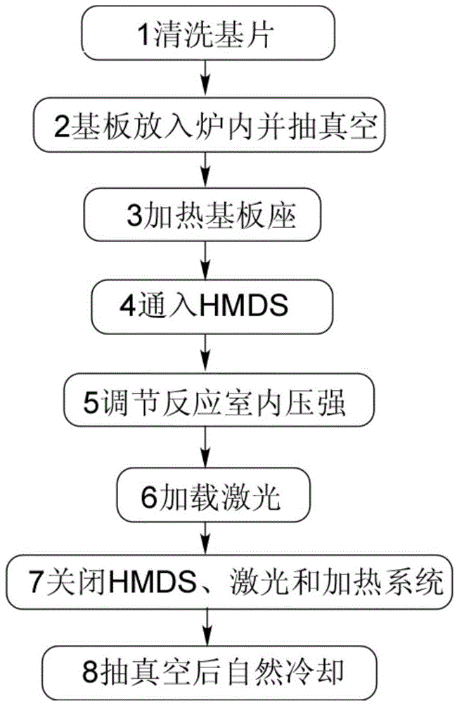
[0026] A method for preparing a cubic silicon carbide film, comprising the steps of:

[0027] (1) Put the monocrystalline silicon substrate on the substrate seat of the cold-wall laser chemical vapor deposition reactor, adjust the vacuum degree to below 10Pa, and set the heating system in the reactor to raise the temperature of the substrate seat to 300°C ;

[0028] (2) The carrier gas Ar gas containing hexamethyldisilane (HMDS) is passed into the reactor, the flow rate of HMDS is 3 sccm, and the vacuum degree in the reactor is 10000Pa by adjusting the vacuum pump exhaust valve;

[0029] (3) load a continuous laser to irradiate the surface of the silicon substrate, the wavelength is 808 nanometers, the laser power is adjusted to 80W, and the laser loading time is 10 minutes;

[0030] (4) Stop feeding the Ar gas containing HMDS, turn off the laser and the heating system in the reactor, evacuate, adjust the vacuum in the reactor to below 10Pa, and naturally cool to room tempera...

Embodiment 2

[0036] A method for preparing a cubic silicon carbide film, comprising the steps of:

[0037] (1) Put the monocrystalline silicon substrate on the substrate seat of the cold-wall laser chemical vapor deposition reactor, adjust the vacuum degree to below 10Pa, and set the heating system in the reactor to raise the temperature of the substrate seat to 600°C ;

[0038] (2) The carrier gas Ar gas containing hexamethyldisilane (HMDS) is passed into the reactor, the flow rate of HMDS is 10 sccm, and the vacuum degree in the adjustment reactor is 1000Pa;

[0039](3) load a continuous laser to irradiate the surface of the silicon substrate, the wavelength is 1080 nanometers, the laser power is adjusted to 20W, and the laser loading time is 3 minutes;

[0040] (4) Stop feeding the H containing HMDS 2 , turn off the laser and the heating system in the reactor, evacuate, adjust the vacuum in the reactor to below 10Pa, and cool naturally to room temperature to obtain a cubic silicon car...

Embodiment 3

[0043] A method for preparing a cubic silicon carbide film, comprising the steps of:

[0044] (1) Put the monocrystalline silicon substrate on the substrate seat of the cold-wall laser chemical vapor deposition reactor, adjust the vacuum degree to below 10Pa, and set the heating system in the reactor to raise the temperature of the substrate seat to 900°C ;

[0045] (2) The carrier gas H containing hexamethyldisilane (HMDS) 2 Pass in the reactor, the flow rate of HMDS is 18sccm, and the vacuum degree in the adjustment reactor is 100Pa;

[0046] (3) Loading a continuous laser to irradiate the surface of the silicon substrate, the laser wavelength is 1080 nanometers, the laser power is adjusted to 150W, and the laser loading time is 1 minute;

[0047] (4) Stop feeding the carrier gas H containing HMDS 2 , turn off the laser and the heating system in the reactor, evacuate, adjust the vacuum in the reactor to below 10Pa, and cool naturally to room temperature to obtain a cubic ...


PUM


Abstract

The invention discloses a preparation method of a cubic silicon carbide film. The preparation method comprises the following steps of (1) placing a monocrystalline silicon substrate on a substrate seat of a cold-wall type laser induced chemical vapor deposition device, vacuumizing, and heating the substrate seat to 100-900 DEG C; (2) introducing HMDS-containing carrier gas to a reactor and regulating the vacuum degree to 10-10000Pa, wherein the flux of HMDS is 1-20sccm; (3) loading continuous laser to irradiate the surface of the silicon substrate at the wavelength of 750-1150nm and the power of 10-150W for 1-10min; (4) stopping the introduction of the HMDS-containing carrier gas, closing the laser, stopping heating, vacuumizing, and naturally cooling to room temperature to obtain the cubic silicon carbide film. A planar defect of the cubic silicon carbide film prepared by the invention trends to grow towards the growth direction of the film, and the self-disappearance phenomenon can be generated when adjacent defects meet, so that crystal defects in the material are effectively reduced.

Description

technical field [0001] The invention relates to a method for preparing a cubic silicon carbide thin film with reduced crystal defects, and belongs to the field of inorganic material structure control. Background technique [0002] Silicon carbide has a large band gap and high breakdown voltage, and is suitable for high temperature, high power, high frequency and extreme radiation environments. It is an ideal material for the development of high frequency, high temperature resistant, radiation resistant semiconductor microelectronic devices and circuits. Important third-generation semiconductor materials. [0003] Silicon carbide has a variety of homogeneous polycrystals, and silicon carbide can be divided into more than 200 different polytypes according to the order of atomic stacking in the direction perpendicular to the c-axis. Since the melting point of cubic silicon carbide (3C-SiC) is lower than that of silicon (the melting point of silicon is 1420°C), 3C-SiC is the on...

Claims


Application Information

Patent Timeline
Patent Type & Authority Applications(China)
IPC IPC(8): C23C16/32C23C16/48
Inventor 章嵩徐青芳涂溶张联盟
Owner 武汉拓材科技有限公司
Why Eureka
Try Eureka