Storage cell, formation method of storage cell and reading method of storage cell

A memory unit and special zone technology, applied in static memory, read-only memory, information storage, etc., can solve the problems of limited drive capacity, large chip area, and high process cost, and achieve the goal of reducing drive capacity, improving integration, and reducing costs Effect

Active Publication Date: 2014-10-08
SHANGHAI HUAHONG GRACE SEMICON MFG CORP
View PDF6 Cites 10 Cited by
  • Summary
  • Abstract
  • Description
  • Claims
  • Application Information

AI Technical Summary

Problems solved by technology

For example, the read current of a single memory cell in the erased state is 75 μA. When all 8 memory cells are in the erased state, the selection transistor needs to pass a current of 600 μA. Such a current requires a large drive capacity Transistors are used as selection transistors. Due to the large resistance of the selection transistors, the driving capability is limited, which will affect the read performance of the memory cells.
The chip area occupied by the selection transistor with a larger driving capability is also larger, resulting in a larger area occupied by the peripheral circuit of the memory, resulting in a lower integration of the memory and higher process costs.
[0007] Therefore, the process cost of the memory needs to be further reduced

Method used


Image

  • Storage cell, formation method of storage cell and reading method of storage cell
  • Storage cell, formation method of storage cell and reading method of storage cell
  • Storage cell, formation method of storage cell and reading method of storage cell

Examples


Embodiment Construction

[0025] As mentioned in the background, the process cost of the memory needs to be further reduced.

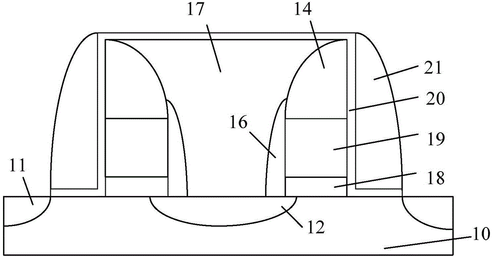
[0026] Research has found that the process cost of memory is affected by the degree of memory integration. The higher the degree of memory integration, the greater the number of memories that can be formed on a single wafer, and the lower the memory process cost. In the prior art, the chip area occupied by the selection transistor connected to the source terminal of the memory unit is generally large, so that the selection transistor has a relatively large driving capability and meets the requirements of the read operation of the memory, but the volume of the selection transistor If it is large, the integration degree of the memory will be reduced, which is not conducive to the reduction of the process cost of the memory.

[0027] In order to reduce and solve the above problems, an embodiment of the present invention provides a memory cell and its forming method and driving met...


PUM


Abstract

The invention discloses a storage cell, a formation method of the storage cell and a reading method of the storage cell. The formation method of the storage cell comprises the steps that a semiconductor substrate is provided, wherein the semiconductor substrate comprises a first bit area and a second bit area, and a first dielectric layer, a floating gate material layer and a second dielectric layer are formed on the surface of the semiconductor substrate; a first doping area is formed in the first bit area; a second doping area is formed in the second bit area, wherein the dosage concentration of the second doping area is smaller than that of the first doping area; the second dielectric layer is etched to form an opening; a side wall is formed on the surface of the side wall of the opening; the floating gate material layer and the first dielectric layer are etched with the side wall as a mask to the surface of the semiconductor substrate; a source line is formed in the opening; the second dielectric layer and the floating gate material layer and the first dielectric layer below the second dielectric layer are removed, and a floating gate and a floating gate dielectric layer below the side wall are formed; a tunneling dielectric layer is formed; a word line located on the surface of the tunneling dielectric layer is formed; a first drain area and a second drain area are formed. The formation method of the storage cell can lower the cost of a storage.

Description

technical field [0001] The invention relates to the technical field of semiconductors, in particular to a memory unit, a forming method and a reading method thereof. Background technique [0002] Electrically Erasable Programmable Read-Only Memory (EEPROM) is a long-life non-volatile memory (it can still maintain the stored data information in the case of power failure). Under normal circumstances, the stored information can be kept for a long time, and it has many advantages such as high integration, fast access speed and easy erasure, so it has been widely used in many fields such as microcomputers and automatic control. The electrically erasable programmable read-only memory takes Byte (8bit) as the minimum modification unit to perform operations such as reading, erasing, and modifying. [0003] Please refer to figure 1 , is a schematic structural diagram of an existing electrically erasable programmable read-only memory unit. [0004] The EEPROM unit includes: a semic...

Claims


Application Information

Patent Timeline
Patent Type & Authority Applications(China)
IPC IPC(8): H01L27/115H01L21/8247G11C16/02
Inventor 于涛
Owner SHANGHAI HUAHONG GRACE SEMICON MFG CORP
Why Eureka
Try Eureka