
High-gain and low-noise differential trans-impedance amplifier
A transimpedance amplifier and low-noise technology, applied in the field of high-gain and low-noise differential transimpedance amplifiers, can solve problems such as small bandwidth, high noise, and insufficient gain, and achieve fewer tubes, reduced power consumption, and reduced chip area Effect
Patent Information
- Authority / Receiving Office
- CN · China
- Current Assignee / Owner
- Publication Date
- 2014-10-22
Smart Images
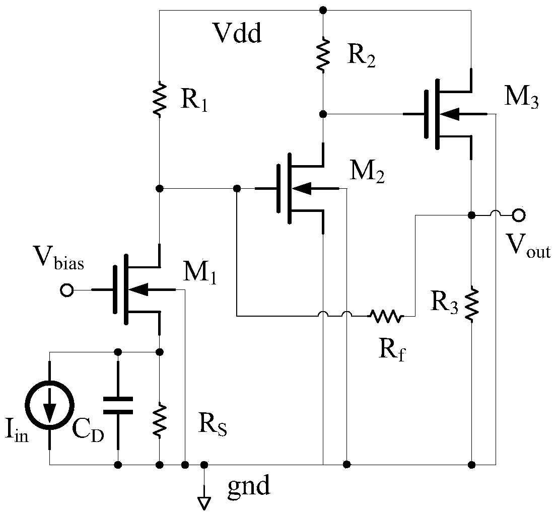
Figure 1 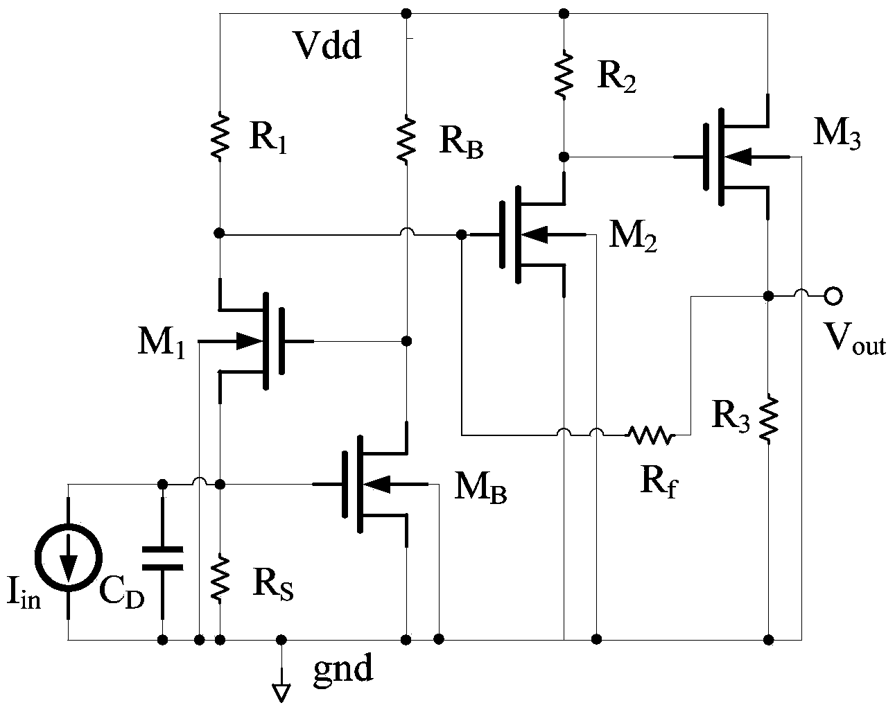
Figure 2 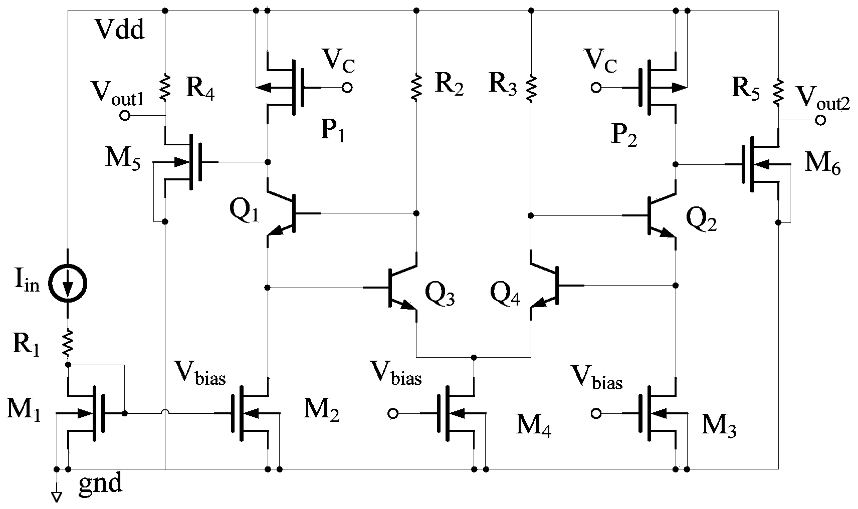
Figure 3
Abstract
Description
technical field
[0001] The invention relates to the field of integrated circuits, in particular to a high-gain, low-noise differential transimpedance amplifier. Background technique
[0002] In fiber optic communication systems, preamplifiers have a significant impact on the performance of the entire system, such as speed, sensitivity, and signal-to-noise ratio. According to the characteristics of the bias resistor, there are three optional preamplifiers: low impedance amplifier, transimpedance amplifier and high impedance amplifier. Low-impedance amplifiers have simple structure and large bandwidth, but the gain is not high enough, and the noise is large, while high-impedance amplifiers have high sensitivity and low noise, but have the disadvantages of small bandwidth and narrow dynamic range. Choosing a transimpedance amplifier can meet these performance requirements A good compromise was achieved.
[0003] Such as figure 1 Shown is the structure diagram of the current-...
Examples
Embodiment Construction
[0044] In order to make the technical problems, technical solutions and advantages to be solved by the present invention clearer, the following will describe in detail with reference to the drawings and specific embodiments.
[0045] Such as figure 2 Shown is the circuit diagram of the RGC (Regulated-Cascade, adjusted cascode) transimpedance amplifier.
[0046] exist figure 2 Among them, Vdd is the power supply voltage, gnd is the ground terminal, I in is the input current signal, C D is the photodetector parasitic capacitance, V out is the output voltage signal;
[0047] and figure 1 Compared with the current-mode form transimpedance amplifier structure shown, figure 2 The RGC transimpedance amplifier shown adds the NMOS transistor M B and resistor R B A common source amplifier is used as a negative feedback path, and the NMOS transistor M 1 Provide bias voltage; if M 1 The drain-source current increases, the resistor R S The voltage drop increases, that is, the...