Integrated nonpolar GaN nanowire transistor high in electron mobility and preparation method thereof

A technology with high electron mobility and nanowires, which is applied in the direction of nanotechnology, nanotechnology, semiconductor/solid-state device manufacturing, etc., can solve the problems of uneven arrangement of nanowires, low yield, disorder, etc., and achieve uncontrollable Sexuality and disorder, optimization of process methods, and simplification of process steps

Active Publication Date: 2014-10-29
JIANGSU INST OF ADVANCED SEMICON CO LTD
View PDF2 Cites 17 Cited by
  • Summary
  • Abstract
  • Description
  • Claims
  • Application Information

AI Technical Summary

Problems solved by technology

This preparation technology separates the nanowire epitaxial growth from the device preparation, which increases the complexity of the process
Nanowires are transferred by coating w...

Method used


Image

  • Integrated nonpolar GaN nanowire transistor high in electron mobility and preparation method thereof
  • Integrated nonpolar GaN nanowire transistor high in electron mobility and preparation method thereof
  • Integrated nonpolar GaN nanowire transistor high in electron mobility and preparation method thereof

Examples


preparation example Construction

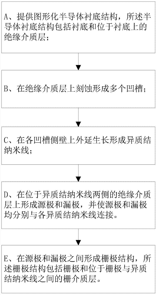
[0041] reference image 3 , The preparation method of integrated non-polar GaN nanowire high electron mobility transistor includes the following steps:

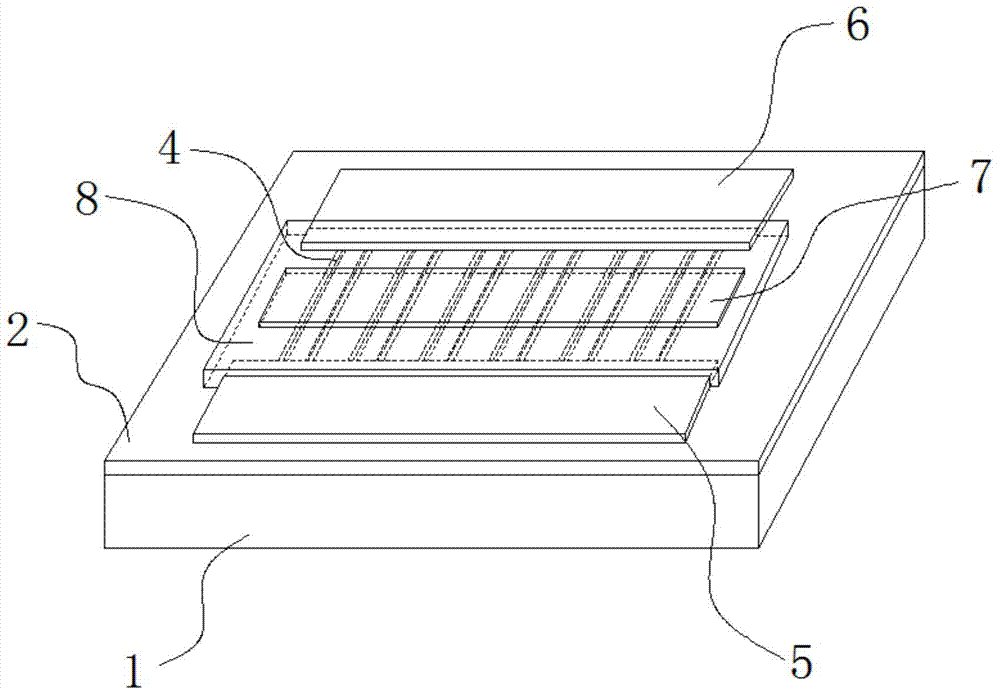
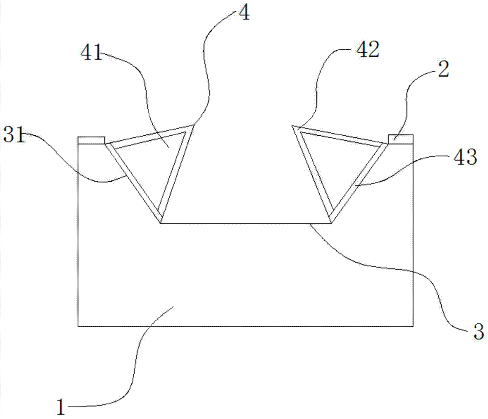
[0042] A. Provide a patterned semiconductor substrate 1 structure, the semiconductor substrate 1 structure includes a substrate 1 and an insulating dielectric layer 2 on the substrate 1;

[0043] B. A plurality of grooves 3 are formed by etching on the insulating dielectric layer 2;

[0044] C. Epitaxially grow the heterojunction nanowire 4 on the sidewall 31 of each groove 3;

[0045] D. Form a source 5 and a drain 6 on the insulating dielectric layer 2 located on both sides of the heterojunction nanowire 4, and connect the source 5 and the drain 6 to each heterojunction nanowire 4 respectively;

[0046] E. A gate 7 structure is formed between the source 5 and the drain 6, and the gate 7 structure includes a gate 7 and a gate dielectric layer 8 between the gate 7 and the heterojunction nanowire 4.

[0047] As a further improvement of t...

Embodiment 1

[0054] Example 1, combined reference Figure 1 ~ Figure 3 , Step A is performed to provide a semiconductor substrate 1 structure. The semiconductor substrate 1 structure includes a substrate 1 and an insulating dielectric layer 2 on the substrate 1. The material of the substrate 1 is monocrystalline silicon; the material of the insulating dielectric layer 2 on the substrate 1 is a silicon dioxide layer or silicon nitride, but it is not limited to these two dielectric layers, and may be well-known to those skilled in the art Other dielectric layers. The semiconductor substrate 1 is patterned to form an array of rectangular grooves 3. The rectangular grooves 3 forming the array include: coating a photoresist layer on the surface of the silicon dioxide layer; defining an array of rectangular grooves 3 pattern on the photoresist layer; and wet etching the silicon dioxide Layer; remove the photoresist; wet etch the bottom surface of the groove 3 and the side wall 31 of the groove ...

Embodiment 2

[0058] Example 2, combined reference Figure 1 ~ Figure 3 , Provide a semiconductor substrate 1 structure, the semiconductor substrate 1 structure includes a substrate 1, an insulating dielectric layer 2 located on the substrate 1. The material of the substrate 1 is single crystal silicon, and the material of the insulating dielectric layer 2 on the substrate 1 is a silicon dioxide layer or silicon nitride, but it is not limited to these two dielectric layers, and may be well-known to those skilled in the art. Other dielectric layers. The semiconductor substrate 1 is patterned to form an array of rectangular grooves 3. The rectangular grooves 3 forming the array include: coating a photoresist layer on the surface of the silicon dioxide layer; defining an array of rectangular grooves 3 pattern on the photoresist layer; and wet etching the silicon dioxide Layer; remove the photoresist; wet etch the bottom surface of the groove 3 and the side wall 31 of the groove 3. The patter...


PUM

PropertyMeasurementUnit
Horizontal sizeaaaaaaaaaa

Abstract

The invention discloses an integrated nonpolar GaN nanowire transistor high in electron mobility and a preparation method thereof. The transistor comprises a substrate and an insulating dielectric layer located on the substrate, a plurality of grooves at intervals are etched in the insulating dielectric layer, heterojunction nanowires are respectively grown in the grooves, a source electrode and a drain electrode are formed on the insulating dielectric layer and are respectively located at two ends of the heterojunction nanowires and respectively connected with each heterojunction nanowire, a gate electrode is formed between the source electrode and the drain electrode, and a gate dielectric layer is arranged between the gate electrode and the heterojunction nanowires. According to the transistor, epitaxial growth and device preparation are united organically, process steps are greatly simplified, and the method is simplified. The transistor solves the problem of uncontrollability and disorder caused by the solution dilution and coating for current nanowire transistors, the nanowire transistor preparation success rate is effectively improved. The nanowire transistor can be widely applied to the field of semiconductors.

Description

Technical field [0001] The invention relates to the technical field of semiconductor devices, in particular to an integrated non-polar GaN nanowire high electron mobility transistor and a preparation method thereof. Background technique [0002] Microelectronic integrated circuits and technology are the key factors and core technologies for the rapid development of modern electronic information technology. With the development of microelectronic integration technology, the integration degree of microelectronic devices based on Si materials is getting higher and higher, and the feature size requirements of the devices are getting smaller and smaller. When the minimum feature size is 10nm, the physical limit of microelectronic devices is reached, and Mohr's law no longer holds. This is because nano-semiconductor devices that reach this size have different working mechanisms, materials, and process technologies from microelectronic devices. [0003] Nanoelectronic devices are called...

Claims


Application Information

Patent Timeline
IPC IPC(8): H01L29/778H01L21/335B82Y10/00
CPCH01L29/0669H01L29/66462H01L29/7786
Inventor 李述体李凯于磊王幸福
Owner JIANGSU INST OF ADVANCED SEMICON CO LTD
Why Eureka
Try Eureka