Measuring method for current carrier concentration in solar energy level monocrystal silicon

A carrier concentration, solar-level technology, applied in the direction of measuring devices, single semiconductor device testing, instruments, etc., can solve the problem of carrier mobility decline and other issues

Inactive Publication Date: 2014-11-12
ZHEJIANG UNIV
View PDF4 Cites 8 Cited by
  • Summary
  • Abstract
  • Description
  • Claims
  • Application Information

AI Technical Summary

Problems solved by technology

For example, the silicon raw material purified by physical metallurgy contains high concentrations of impurities such as boron and phosphorus at the same time. There is a boron and phosphorus compensat

Method used


Image

  • Measuring method for current carrier concentration in solar energy level monocrystal silicon
  • Measuring method for current carrier concentration in solar energy level monocrystal silicon
  • Measuring method for current carrier concentration in solar energy level monocrystal silicon

Examples


Embodiment 1

[0051] (1) Select a series of p-type electronic grade single crystal silicon as standard samples, the resistivity of the standard samples is 0.05-50Ω.cm, and the resistivity of the standard samples is evenly distributed within the range of each resistivity magnitude. The standard sample has a uniform thickness of 1-2mm.

[0052] (2) After the standard sample is cleaned by the standard cleaning process, the resistivity of each sample is measured at room temperature according to the national standard "Method for Determination of Resistivity of Silicon Single Crystal" (GB / T1551-2009), and the resistivity is calculated by formula (5) Converted to the corresponding carrier concentration.

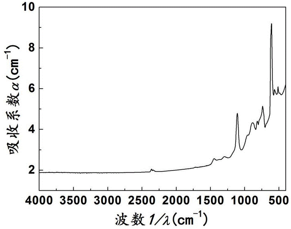
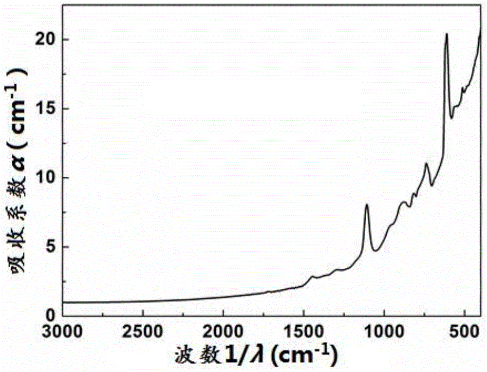
[0053] (3) The standard sample is chemically polished to make the two surfaces mirror, and after being cleaned by a standard cleaning process, the infrared transmission coefficient of each sample is measured by a Fourier transform infrared spectrometer (FTIR), and converted into an infrared trans...

Embodiment 2

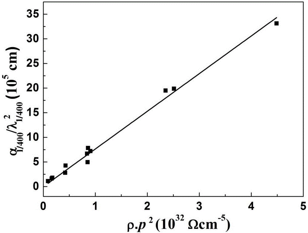
[0061] Steps (1)~(3) are the same as in Example 1, and the (α λ1 -α λ2 ) / (λ 1 2 -λ 2 2 ) and ρp 2 The standard curve of , where: λ 1 = 1 / 400cm, λ 2 = 1 / 1150cm, α λ1 with alpha λ2 are the wavelength λ 1 , lambda 2 The infrared absorption coefficient of the standard sample, such as Figure 4 As shown, its expression is: (α λ1 -α λ2 ) / (λ 1 2 -λ 2 2 )=(α 1 / 400 -α 1 / 1150 ) / (λ 2 1 / 400 - / λ 2 1 / 1150 )=7.9×10 -27 ρp (9)

[0062] For a certain boron-phosphorus compensation type solar-grade monocrystalline silicon sample to be tested in Example 1, its carrier concentration is calculated according to formula (9) to be 2.63×10 16 cm -3 . As a preferred method, the result is more accurate than Example 1.

[0063] It can be seen that the carrier concentration in solar-grade monocrystalline silicon can be measured more accurately by using the method of the present invention.


PUM

PropertyMeasurementUnit
Resistivityaaaaaaaaaa
Thicknessaaaaaaaaaa
Resistivityaaaaaaaaaa

Abstract

The invention discloses a measuring method for the current carrier concentration in solar energy level monocrystal silicon. The measuring method includes the following steps that (1), a series of p-type electronic grade monocrystal silicon and a series of n-type electronic grade monocrystal silicon are respectively selected as standard samples, the electrical resistivity and infrared absorption coefficients of the standard samples are respectively measured at the room temperature, and the corresponding current carrier concentration is converted according to the electrical resistivity; (2), according to measurement results in the step (1), an alpha lambda/ lambda<2> and rho p<2> standard curve of the p-type monocrystal silicon and an alpha lambda/ lambda<2> and rho p<2> standard curve of the n-type monocrystal silicon are respectively set up, wherein alpha lambda is the infrared absorption coefficients of the standard samples at the wavelength of lambda, and p and rho are the corresponding current carrier concentration and the corresponding electrical resistivity; (3), the electric conduction type of the solar energy level monocrystal silicon samples to be detected is determined, the electrical resistivity and the infrared absorption coefficients of the standard samples are respectively measured at the room temperature, and the current carrier concentration is obtained according to the corresponding standard curves in the step (2). The measuring method is easy, convenient and fast to use, high in accuracy, low in test cost and particularly suitable for the solar energy level monocrystal silicon, wherein the compensation effect exists in a substrate of the solar energy level monocrystal silicon.

Description

technical field [0001] The invention relates to the detection of characteristic parameters of semiconductor materials, in particular to a method for measuring carrier concentration in solar-grade monocrystalline silicon. Background technique [0002] The electrons and holes that can conduct electricity in semiconductor materials are called carriers, and the carrier concentration is a basic parameter of optoelectronic materials, which has an extremely important impact on electrical properties. In semiconductor materials, the type and concentration of doped impurities are often controlled to control the carrier concentration in the material, and finally achieve the purpose of controlling the electrical properties of the material. Solar-grade semiconductor materials have high requirements for material purity, carrier mobility, and light absorption coefficient. The monitoring and control of carrier concentration and distribution in semiconductors is a key point in the manufactu...

Claims


Application Information

Patent Timeline
IPC IPC(8): G01R31/26G01N27/04G01N21/3563
Inventor 余学功陈鹏杨德仁
Owner ZHEJIANG UNIV
Why Eureka
Try Eureka