GaN thin film growing on W substrate, as well as preparation method and application thereof

A substrate and thin film technology, applied in the field of GaN thin film and its preparation, can solve the problems affecting the growth of epitaxial thin film, difficulty in thin film epitaxy, unstable chemical properties of metal W substrate, etc. Excellent effect of nuclear time and singleness

Inactive Publication Date: 2014-11-19
SOUTH CHINA UNIV OF TECH
View PDF6 Cites 2 Cited by
  • Summary
  • Abstract
  • Description
  • Claims
  • Application Information

AI Technical Summary

Problems solved by technology

[0006] However, the chemical properties of the metal W substrate are unstable at high temperatures. When the epitaxial temperature is higher than 600 ° C, the interface reaction between the epitaxial nitride and the metal substrate will seriously affect the quality of the epitaxial film growth.
Pioneering researcher and well-known scientist Akasaki et al. have tried to apply traditional MOCVD or MBE technology to directly epitaxially grow nitrides on substrate materials with variable chemical properties. difficulty

Method used


Image

  • GaN thin film growing on W substrate, as well as preparation method and application thereof
  • GaN thin film growing on W substrate, as well as preparation method and application thereof
  • GaN thin film growing on W substrate, as well as preparation method and application thereof

Examples


Embodiment 1

[0043] The preparation method of the GaN thin film grown on the W substrate of the present embodiment comprises the following steps:

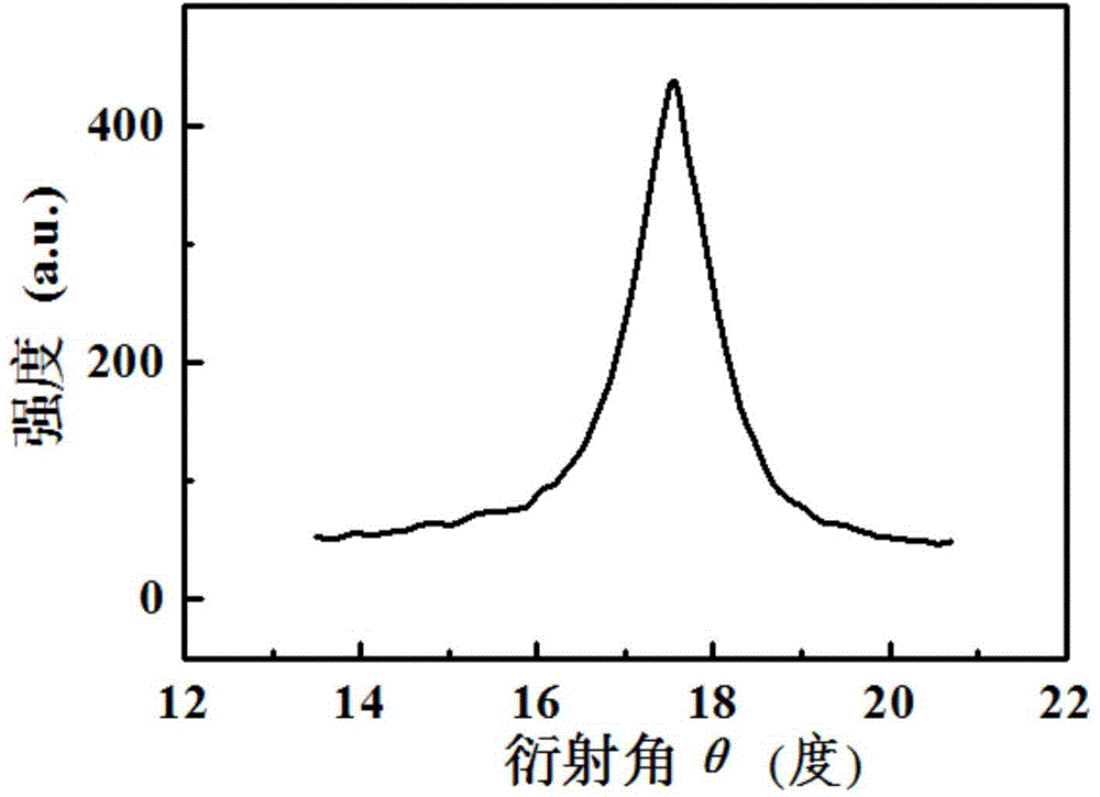
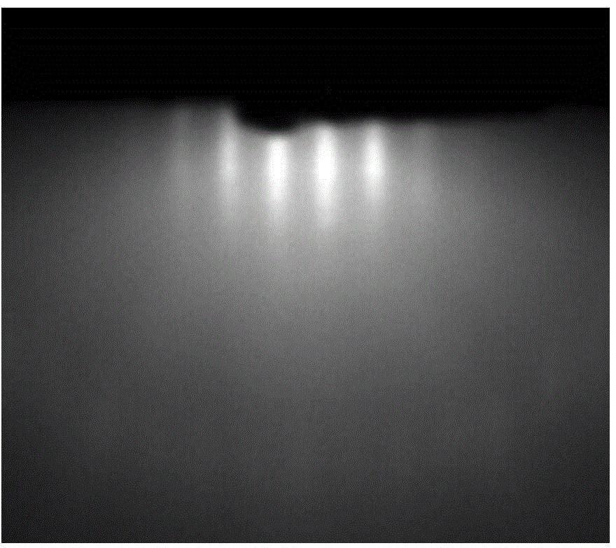
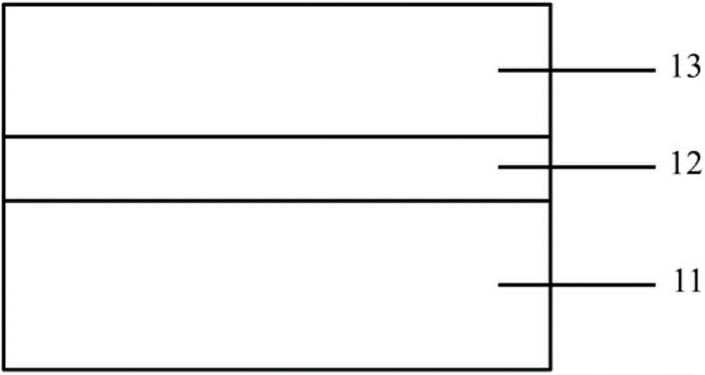
[0044] (1) Selection of the substrate and its crystal orientation: the epitaxial substrate adopts the (0001) plane of the W substrate as the epitaxial plane, and the selected crystal epitaxial orientation relationship: GaN(0001) / / W(0001).

[0045] (2) Substrate surface polishing, cleaning and annealing treatment, the specific process of the annealing is: put the substrate W under a pressure of 2×10 -10 In the growth chamber of Torr's UHV-PLD, bake at a high temperature of 900 °C for 1 hour, and then air cool to 400 °C.

[0046] The surface polishing of the substrate is specifically:

[0047] First, the surface of the substrate is polished with diamond slurry, and the surface of the substrate is observed with an optical microscope until there are no scratches, and then the chemical mechanical polishing method is used for polishing.

[0048] Th...

Embodiment 2

[0057] The preparation method of the GaN thin film grown on the W substrate of the present embodiment comprises the following steps:

[0058] (1) Selection of the substrate and its crystal orientation: the (110) plane of the W substrate is used as the epitaxial plane, and the crystal epitaxial orientation relationship: AlN[11-20] / / W[001];

[0059] (2) Carrying out surface polishing, cleaning and annealing treatment to the substrate;

[0060] The surface polishing is specifically:

[0061] The surface of the W substrate is polished with diamond slurry, and the surface of the substrate is observed with an optical microscope until there are no scratches, and then the chemical mechanical polishing method is used for polishing;

[0062] The cleaning is specifically:

[0063] Put the W substrate in deionized water and ultrasonically clean it at room temperature for 3 minutes to remove the sticky particles on the surface of the W substrate, then wash it with hydrochloric acid, acet...

Embodiment 3

[0070] The preparation method of the GaN thin film grown on the W substrate of the present embodiment comprises the following steps:

[0071] (1) Selection of the substrate and its crystal orientation: the (110) plane of the W substrate is used as the epitaxial plane, and the crystal epitaxial orientation relationship: AlN[11-20] / / W[001];

[0072] (2) Carrying out surface polishing, cleaning and annealing treatment to the substrate;

[0073] The surface polishing is specifically:

[0074] The surface of the W substrate is polished with diamond slurry, and the surface of the substrate is observed with an optical microscope until there are no scratches, and then the chemical mechanical polishing method is used for polishing;

[0075] The cleaning is specifically:

[0076] Put the W substrate in deionized water and ultrasonically clean it at room temperature for 5 minutes to remove the sticky particles on the surface of the W substrate, then wash it with hydrochloric acid, acet...


PUM

PropertyMeasurementUnit
thicknessaaaaaaaaaa
thicknessaaaaaaaaaa
thicknessaaaaaaaaaa

Abstract

The invention discloses a GaN thin film growing on a W substrate. The GaN thin film comprises an AlN buffer layer growing on the W substrate and a GaN thin film growing on the AlN buffer layer; the AlN buffer layer is an AlN buffer layer growing at 400-500 GEG C; the GaN thin film is a GaN thin film growing at 700-800 DEG C. The invention further discloses a preparation method and application for the GaN thin film growing on the W substrate. The GaN thin film growing on the W substrate prepared by the method has the advantages of low dislocation density and high crystal quality.

Description

technical field [0001] The invention relates to a GaN thin film and a preparation method thereof, in particular to a GaN thin film grown on a W substrate and a preparation method thereof. Background technique [0002] Light-emitting diode (LED), as a new type of solid-state lighting source and green light source, has outstanding features such as small size, low power consumption, environmental protection, long service life, high brightness, low heat and colorful, and is widely used in outdoor lighting, commercial lighting and decoration Engineering and other fields have a wide range of applications. At present, under the background of the increasingly serious problem of global warming, saving energy and reducing greenhouse gas emissions has become an important issue faced by the whole world. A low-carbon economy based on low energy consumption, low pollution, and low emissions will become an important direction of economic development. In the field of lighting, the applica...

Claims


Application Information

Patent Timeline
Patent Type & Authority Applications(China)
IPC IPC(8): H01L33/02H01L33/12
CPCH01L33/12H01L33/007H01L33/16
Inventor 李国强王文樑刘作莲杨为家林云昊周仕忠钱慧荣
Owner SOUTH CHINA UNIV OF TECH
Why Eureka
Try Eureka