
Design method for large-bandwidth strong-absorption metamaterial near-infrared wave-absorbing material

A wave-absorbing material and design method technology, applied in optical components, optics, instruments, etc., can solve problems such as narrow absorption bandwidth and limit the application of devices, and achieve the effects of rapid production, widening absorption bandwidth, and improving conversion efficiency

Inactive Publication Date: 2014-12-03
ZHEJIANG UNIV
View PDF2 Cites 18 Cited by
  • Summary
  • Abstract
  • Description
  • Claims
  • Application Information

AI Technical Summary

Problems solved by technology

[0005] Metamaterial wave absorption is generally based on electric and magnetic resonance, which makes the general perfect absorption bandwidth relatively narrow, which limits the actual device application

Method used


Image

  • Design method for large-bandwidth strong-absorption metamaterial near-infrared wave-absorbing material
  • Design method for large-bandwidth strong-absorption metamaterial near-infrared wave-absorbing material
  • Design method for large-bandwidth strong-absorption metamaterial near-infrared wave-absorbing material

Examples


Embodiment Construction

[0029] The present invention will be further described below in conjunction with drawings and embodiments.

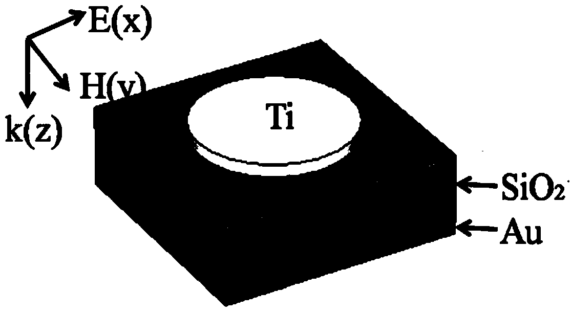
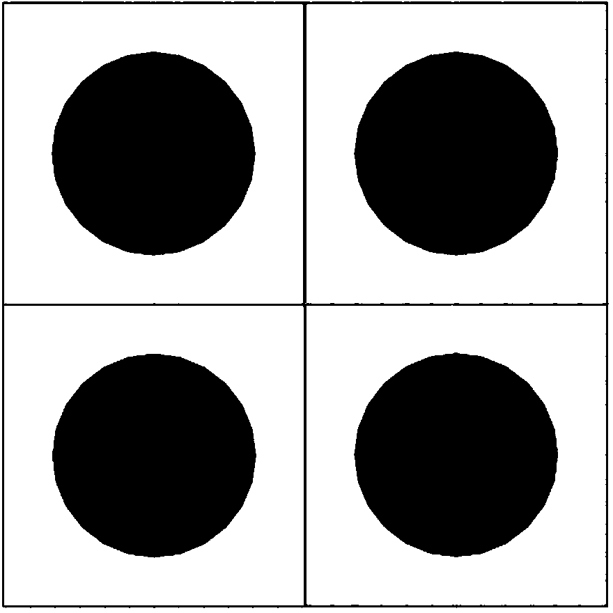
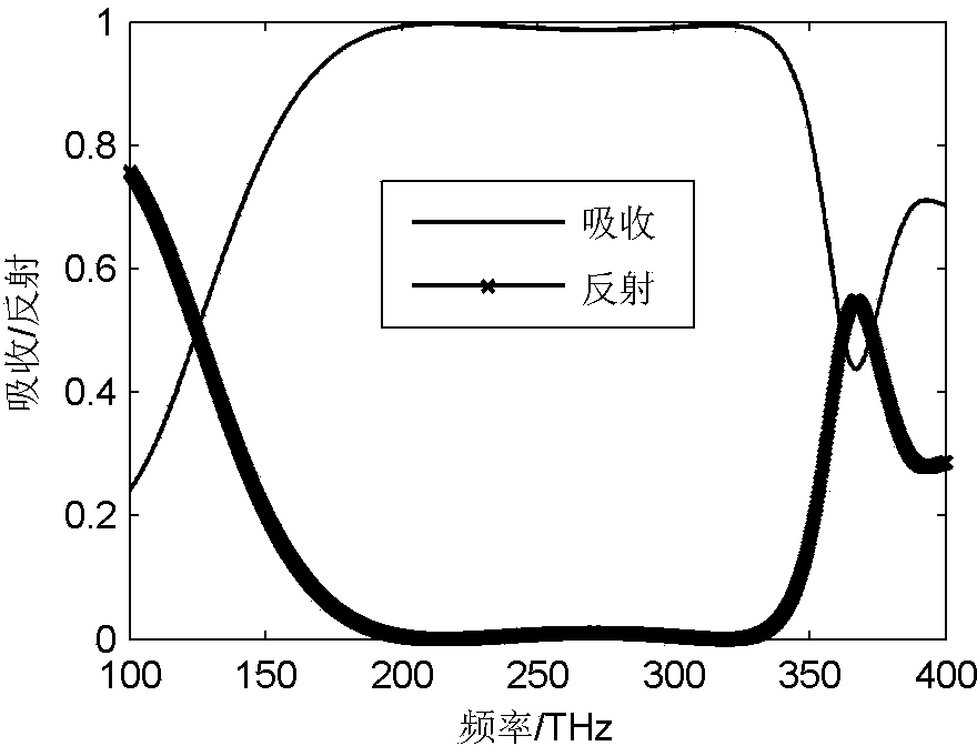
[0030] Such as figure 1 , figure 2 As shown, the metamaterial near-infrared absorbing material is composed of periodic unit structures. Each unit structure is composed of three layers of different materials, each of which has a thickness much smaller than the wavelength. Specifically, a layer of gold film with a thickness of about 100nm is set on the silicon substrate to suppress the transmission of light; on the gold film is a continuous silicon dioxide film with a thickness of 160nm; the uppermost layer is made of metal titanium The resonant disc has a diameter of 400nm and a thickness of 30nm. Among them, the refractive index of silicon dioxide in the near infrared is about 1.45, and the dielectric constant of metal titanium is represented by the Drude model. The plasma frequency of gold is 1.366×10 16 Hz, the collision frequency is 1.2×10 14 Hz; the plasma fr...


PUM


Abstract

The invention discloses a design method for a large-bandwidth strong-absorption metamaterial near-infrared wave-absorbing material. The method includes the following steps: 1. according to an effective medium theory and through simulation of a CST microwave studio, S parameters are obtained, wherein a frequency domain calculation mode is adopted during the simulation; periodic unit structures are periodically distributed in x and y directions and the periodic distribution is set as a periodic boundary condition; and according to parameters S11 (Omega) and S21(Omega) obtained through scanning, a resistance value is calculated. 2. through change of the period of the unit structures and the sizes of titanium resonant plates, corresponding absorption frequencies are adjusted and then the plurality of resonant plates of different sizes are horizontally placed in one unit so that absorption spectral lines corresponding to the different resonant plates are overlapped. The method adopts a high-loss metal so that a wideband wave-absorbing effect can be achieved through a simple structure. Resonant units of one size are replaced by the resonant units of different sizes so that a resonance mode of adjacent frequencies can be triggered and an absorption bandwidth can be further expanded.

Description

technical field [0001] The invention belongs to the field of electromagnetic wave absorption and radiation control, and in particular relates to a design method of a near-infrared wave-absorbing material with a large bandwidth and strong absorption metamaterial. Background technique [0002] Electromagnetic wave absorbing materials refer to a class of functional composite materials that can absorb and attenuate incident electromagnetic wave energy, and convert the electromagnetic energy into heat energy or other energy forms through the dielectric loss of the material. The research of electromagnetic wave absorbing materials is of great significance in the application of military and national economy, and has important applications in many aspects such as radar stealth, thermal radiometer, infrared detector and thermal photovoltaic battery. Traditional conventional electromagnetic wave absorbing materials are based on the conversion of electromagnetic wave energy into therma...

Claims


Application Information

Patent Timeline
Patent Type & Authority Applications(China)
IPC IPC(8): G02B5/00
Inventor 丁飞朱剑飞金毅何赛灵
Owner ZHEJIANG UNIV
Learn More