Hemispheroid solid fluctuation micro-gyroscope and manufacturing method thereof
A technology of micro gyroscopes and hemispheres, applied in gyroscope/steering sensing equipment, gyro effect for speed measurement, instruments, etc., can solve crosstalk, does not reach the megahertz level, and the effective vibration mass is only distributed on the edge of the shell and other issues, to achieve the effect of reducing environmental noise, increasing the effective vibration mass, and reducing mutual crosstalk
- Summary
- Abstract
- Description
- Claims
- Application Information
AI Technical Summary
Problems solved by technology
Method used
Image
Examples
Embodiment 1
[0033] Such as figure 2 As shown, the present embodiment provides a hemispherical solid-state wave micro-gyroscope, comprising:
[0034] a single crystal silicon substrate 1;
[0035] Eight evenly distributed signal electrodes 2;
[0036] Eight evenly distributed shielding electrodes 3;
[0037] A miniature hemispherical resonator 4;
[0038] A central fixed support column 5;
[0039] Among them: the miniature hemispherical resonator 4 is connected to the monocrystalline silicon substrate 1 through the central fixed support column 5; the signal electrode 2 and the shielding electrode 3 are arranged on the upper surface of the monocrystalline silicon substrate 1, and the two are interlaced and evenly distributed on the micro hemisphere Around the bulk resonator 4 , the distances between the eight signal electrodes 2 and the miniature hemispherical resonator 4 are the same, and the distances between the eight shielding electrodes 3 and the micro hemispherical resonator 4 ar...
Embodiment 2
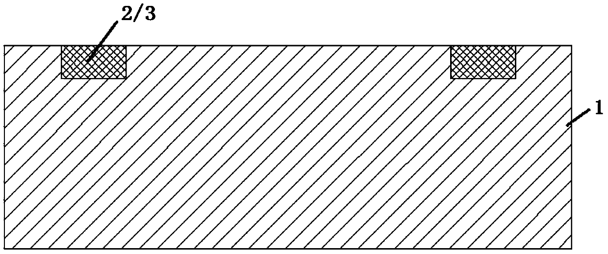
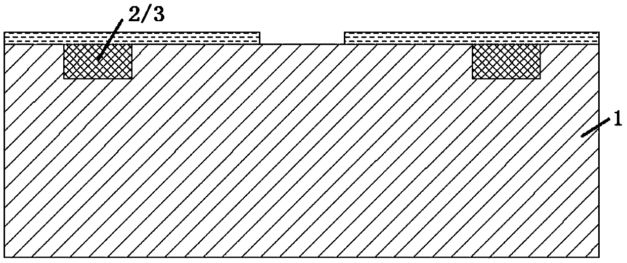
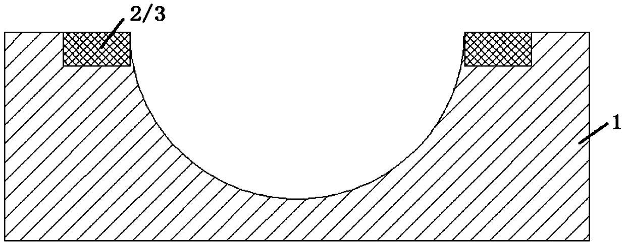
[0048] Such asFigure 1(a)-Figure 1(f) As shown, the present embodiment provides a method for preparing a hemispherical solid-state wave micro-gyroscope, comprising the following steps:
[0049] The first step, as shown in Figure 1(a), is to clean the single crystal silicon substrate 1, apply glue, photolithography, development, boron ion implantation, and degelling process, and obtain a thickness of 10 μm on the single crystal silicon substrate 1. Signal electrode 2 and shielding electrode 3 of 50 μm boron ion-doped silicon material;
[0050] The second step, as shown in Figure 1(b), is to carry out glue coating, photolithography, and development processes on the basis of the first step to obtain a patterned photoresist on the surface of the single crystal silicon substrate 1, which is used for etching the hemisphere shaped groove as a mask;
[0051] The third step, as shown in Fig. 1(c), is to carry out the isotropic etching process and deglue process of single crystal silic...
PUM
| Property | Measurement | Unit |
|---|---|---|
| Thickness | aaaaa | aaaaa |
| Radius | aaaaa | aaaaa |
| Thickness | aaaaa | aaaaa |
Abstract
Description
Claims
Application Information


