Floating junction silicon carbide SBD device with block-shaped groove and buried layer

A silicon carbide and trench technology, applied in the field of microelectronics, can solve the problems of small forward conduction current of the device, low duty cycle of the conduction channel, and reduction of device breakdown voltage, etc., and achieve large forward conduction current , large breakdown voltage and short switching time

Active Publication Date: 2014-12-10
XIDIAN UNIV
View PDF6 Cites 8 Cited by
  • Summary
  • Abstract
  • Description
  • Claims
  • Application Information

AI Technical Summary

Problems solved by technology

[0005] However, the floating junction silicon carbide Schottky diode (SiC FJ-SBD), the buried layer introduced in the epitaxial layer of the device, narrows the conduction channel of the forward conduction current, and the forward conduction current of the device becomes smaller. Conventional The strip-shaped buried layer makes the duty cycle of the conductive channel at the floating junction not high
However, the trench corners of the trenched SiC SBD lead to the peak electric field of the device under the action of the reverse voltage, which reduces the breakdown voltage of the device.

Method used


Image

  • Floating junction silicon carbide SBD device with block-shaped groove and buried layer
  • Floating junction silicon carbide SBD device with block-shaped groove and buried layer
  • Floating junction silicon carbide SBD device with block-shaped groove and buried layer

Examples


Embodiment 1

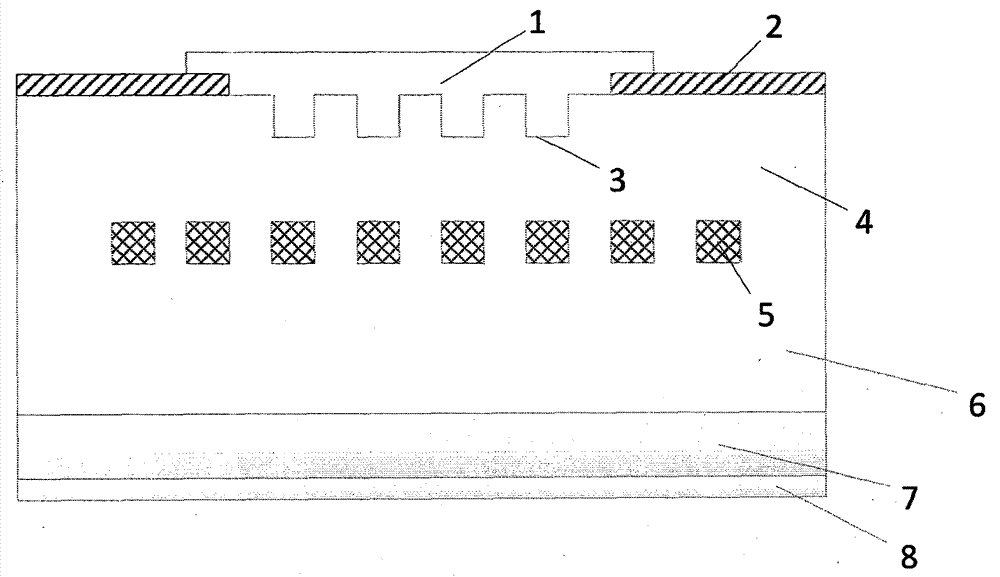
[0046] refer to Figure 1a and Figure 1b , the structure of the trench type floating junction silicon carbide SBD device with circular or hexagonal and elliptical block buried layers in the present invention is as follows:

[0047] N + The substrate is an N-type SiC substrate, and the primary N - The epitaxial layer is located at N + on the substrate, P + The ion-implanted region is located once N - epitaxial layer surface, secondary N - The epitaxial layer is located once N - above the epitaxial layer.

[0048] Metal and SiO 2 The isolation medium is located at the secondary N - Above the epitaxial layer, metal and SiO 2 The isolation dielectric is adjacent, and the metal and SiO 2 There are phase overlaps in the isolation media. The trench is located under the metal, the quadratic N - surface of the epitaxial layer.

[0049] Once N - The thickness of the epitaxial layer is 5 μm, and the doping concentration of nitrogen ions is 1×10 16 cm -3 . P + The dopin...

Embodiment 2

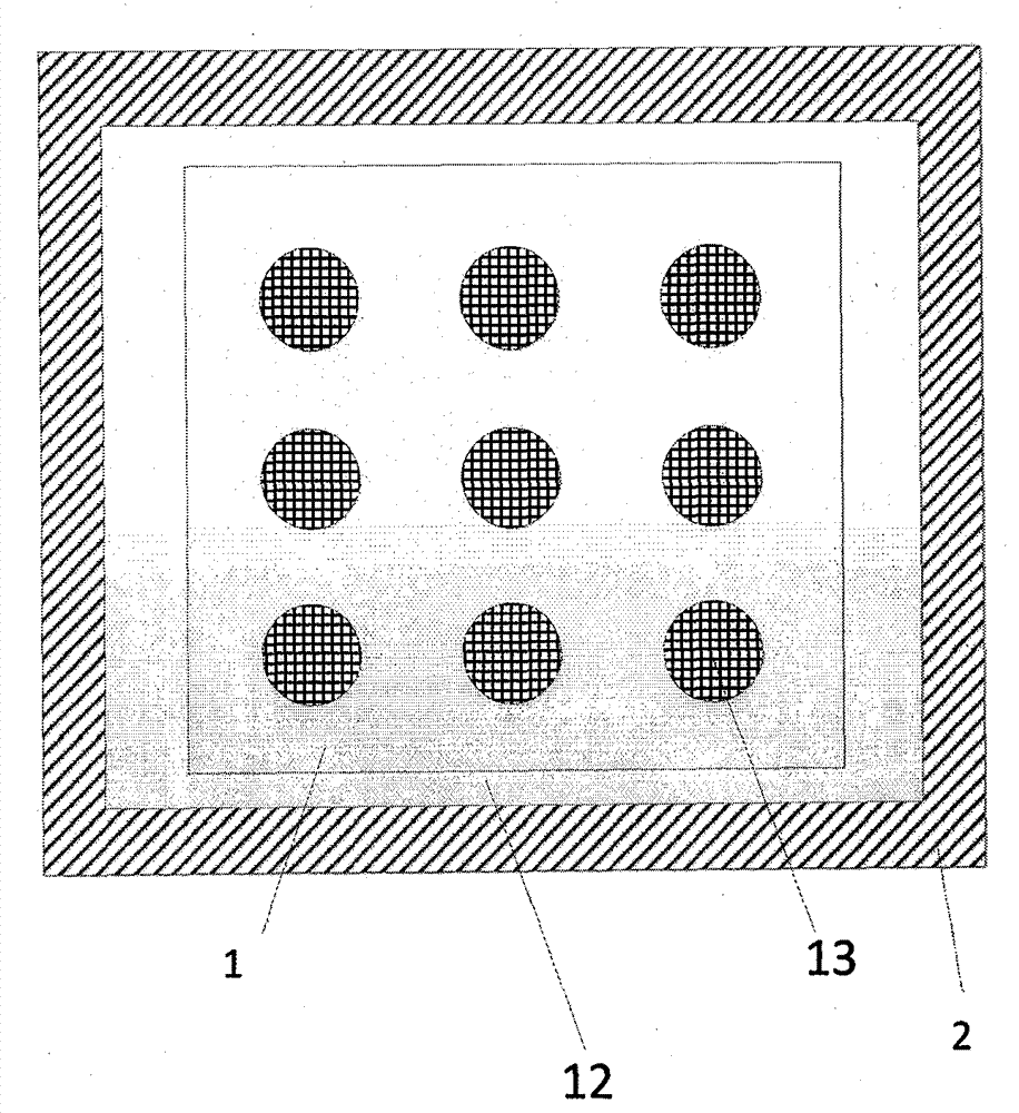
[0053] refer to Figure 1a and Figure 5 , the structure of the trench type floating junction silicon carbide SBD device with circular or hexagonal and elliptical or massive buried layers in the present invention is as follows:

[0054] N + The substrate is an N-type SiC substrate, and the primary N - The epitaxial layer is located at N + on the substrate, P + The ion-implanted region is located once N - epitaxial layer surface, secondary N - The epitaxial layer is located once N - above the epitaxial layer.

[0055] Metal and SiO 2 The isolation medium is located at the secondary N - above the epitaxial layer. Metal and SiO 2 The isolation dielectric is adjacent, and the metal and SiO 2 There are phase overlaps in the isolation media. The trench is located under the metal, the quadratic N - surface of the epitaxial layer.

[0056] Once N - The thickness of the epitaxial layer is 10 μm, and the doping concentration of nitrogen ions is 5×10 15 cm -3 . P + The...

Embodiment 3

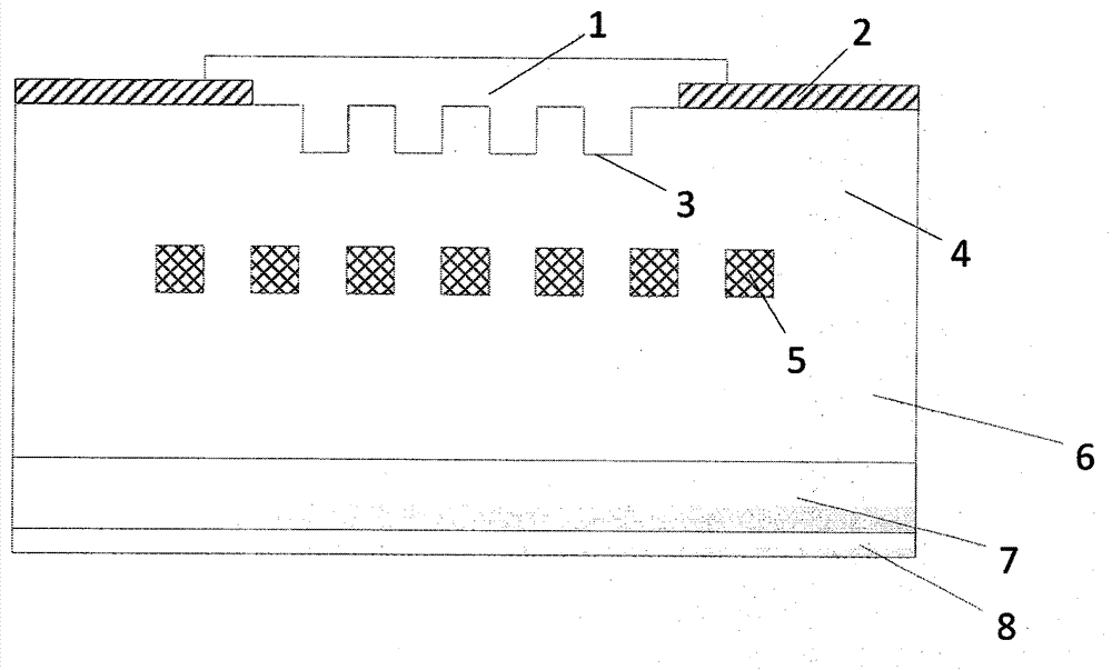
[0060] refer to figure 2 and Figure 8 , the structure of the trench type floating junction silicon carbide SBD device with circular or hexagonal and elliptical block buried layers in the present invention is as follows:

[0061] N + The substrate is an N-type SiC substrate, and the primary N - The epitaxial layer is located at N + on the substrate, P + The ion-implanted region is located once N - epitaxial layer surface, secondary N - The epitaxial layer is located once N - above the epitaxial layer.

[0062] Metal and SiO 2 The isolation medium is located at the secondary N - above the epitaxial layer. Metal and SiO 2 The isolation dielectric is adjacent, and the metal and SiO 2 There are phase overlaps in the isolation media. The trench is located under the metal, the quadratic N - surface of the epitaxial layer.

[0063] Once N - The thickness of the epitaxial layer is 5 μm, and the doping concentration of nitrogen ions is 3×10 15 cm -3 . P + The dopin...


PUM

PropertyMeasurementUnit
depthaaaaaaaaaa
thicknessaaaaaaaaaa
thicknessaaaaaaaaaa

Abstract

The invention relates to a floating junction silicon carbide SBD device with a block-shaped groove and a buried layer. The floating junction silicon carbide SBD device is characterized by comprising a metal, a SiO2 spacer medium, a groove, a primary N- epitaxial layer, a P+ ion injection region, a secondary N- epitaxial layer, an N+ substrate region and an ohmic contact region, wherein the P+ ion injection region is located on the surface of the secondary N- epitaxial layer, the groove is flush with the P+ ion injection region up and down and the groove and the P+ ion injection region are shaped as the same; or a circular, hexagonal or square block-shaped buried layer is taken as a floating junction is flush with the P+ ion injection region up and down and shaped the same as the P+ ion injection region. The floating junction silicon carbide SBD device with the block-shaped groove and the buried layer has either the advantages of large Schottky contact area and large forward on current of a groove-shaped silicon carbide SBD or the advantage of high breakdown voltage of a floating junction silicon carbide SBD.

Description

technical field [0001] The invention relates to the technical field of microelectronics, in particular to a floating junction silicon carbide SBD device with a bulk trench and a buried layer. Background technique [0002] Semiconductor materials have made great leaps in the past few decades. Wide bandgap semiconductor materials are the third-generation semiconductor materials represented by materials such as silicon carbide and gallium nitride. Among them, silicon carbide materials are especially famous. Silicon carbide materials In the 1980s and 1990s, it began to enter people's research sight, and it has developed rapidly in the past ten years. Silicon carbide technology has gradually matured and entered the market, and many silicon carbide technologies have been industrialized. Silicon carbide material has better electrical properties than Si, which makes it very suitable for high voltage, high power and high frequency fields. And its development pace has surpassed othe...

Claims


Application Information

Patent Timeline
Patent Type & Authority Applications(China)
IPC IPC(8): H01L29/872H01L29/06
CPCH01L29/872H01L29/0623H01L29/8725H01L29/0684
Inventor 宋庆文杨帅汤晓燕张艺蒙贾仁需张玉明王悦湖
Owner XIDIAN UNIV
Why Eureka
Try Eureka