
A method for preparing a patterned metal layer on a ceramic surface

A technology of ceramic surface and metal layer, applied in conductive pattern formation and other directions, can solve the problems of reduced reliability of electronic ceramic components, increased process and cost, process chain length, etc., and achieves low production cost, low investment in production equipment, and low cost Simplified effect

Active Publication Date: 2015-12-30
遂宁迪印科技有限公司
View PDF6 Cites 0 Cited by
  • Summary
  • Abstract
  • Description
  • Claims
  • Application Information

AI Technical Summary

Problems solved by technology

Electroplating increases the process and cost, and electroplating has problems such as rough electroplating, copper particles on the electroplating board surface, and electroplating pits, which easily lead to a decrease in the reliability of electronic ceramic components; at the same time, this method deposits a metal layer on the entire ceramic surface. The metal deposition layer needs to be removed by chemical or physical methods, the process chain is long, and the etching process is easy to cause environmental pollution problems

Method used


Image

  • A method for preparing a patterned metal layer on a ceramic surface
  • A method for preparing a patterned metal layer on a ceramic surface
  • A method for preparing a patterned metal layer on a ceramic surface

Examples


Embodiment 1

[0038] A metallized silver layer is prepared on the surface of a ceramic substrate. The ceramic substrate undergoes pretreatments such as descaling, roughening, ultrasonic cleaning, and drying in sequence to obtain a ceramic surface state suitable for printing.

[0039] Configuration 100ml solubility is the palladium ion solution of 0.05mol / L, then adds 100ml of A solution, and finally adds ethanol, ethylene glycol, n-propanol to adjust the viscosity of the solution to be 2mPa·s, surface tension 30mN / m, namely A type I trigger is obtained. The configuration method of solution A is as follows: add 0.12mol hydroxyethyl methacrylate, 0.08mol divinylbenzene and 0.024mol azobisisoheptanonitrile to 200ml ethanol, stir well, take out 180ml solution and place it in a constant pressure drop In the funnel, add 180ml of the solution in the constant pressure dropping funnel dropwise to the remaining 20ml of the original solution within 1 hour. During the dropping process, the temperature...

Embodiment 2

[0042] Prepare the metallization pattern on the surface of capacitor ceramic substrate. The capacitor ceramic substrate undergoes pre-treatments such as descaling, roughening, ultrasonic cleaning, and drying in sequence to obtain a ceramic surface state suitable for printing.

[0043] Configuration 100ml solubility is the palladium ion solution of 0.05mol / L, then adds 10ml of A solution, and finally adds ethanol, ethylene glycol, n-propanol to adjust the viscosity of the solution to be 3mPa·s, and the surface tension is 45mN / m, namely A type I trigger is obtained. The configuration method of solution A is as follows: add 0.12mol hydroxyethyl methacrylate, 0.08mol divinylbenzene and 0.024mol azobisisoheptanonitrile to 200ml ethanol, stir well, take out 180ml solution and place it in a constant pressure drop In the funnel, add 180ml of the solution in the constant pressure dropping funnel dropwise to the remaining 20ml of the original solution within 1 hour. During the dropping...

Embodiment 3

[0046] A metallized nickel layer is prepared on the surface of a ceramic substrate. The ceramic substrate undergoes pretreatments such as descaling, roughening, ultrasonic cleaning, and drying in sequence to obtain a ceramic surface state suitable for printing.

[0047] Dissolve 0.2mol of dimethylaminoborane in 100ml of deionized water, then add ethanol, n-propanol, and isopropanol to adjust the viscosity of the solution to 2.5mPa·s, and the surface tension to 40mN / m, and the trigger type II is obtained. agent. A modified inkjet printer was used to print the trigger agent on the area to be metallized, and then the pattern was cured at 70°C to obtain a patterned trigger layer.

[0048] Put the ceramic substrate printed with the trigger agent into the metal nickel ion solution to carry out constrained chemical deposition of nickel layer. The temperature of the metal nickel ion solution is 40° C., the pH is 9, and the time for constrained chemical deposition is 15 minutes. The...


PUM

PropertyMeasurementUnit
viscosityaaaaaaaaaa

Abstract

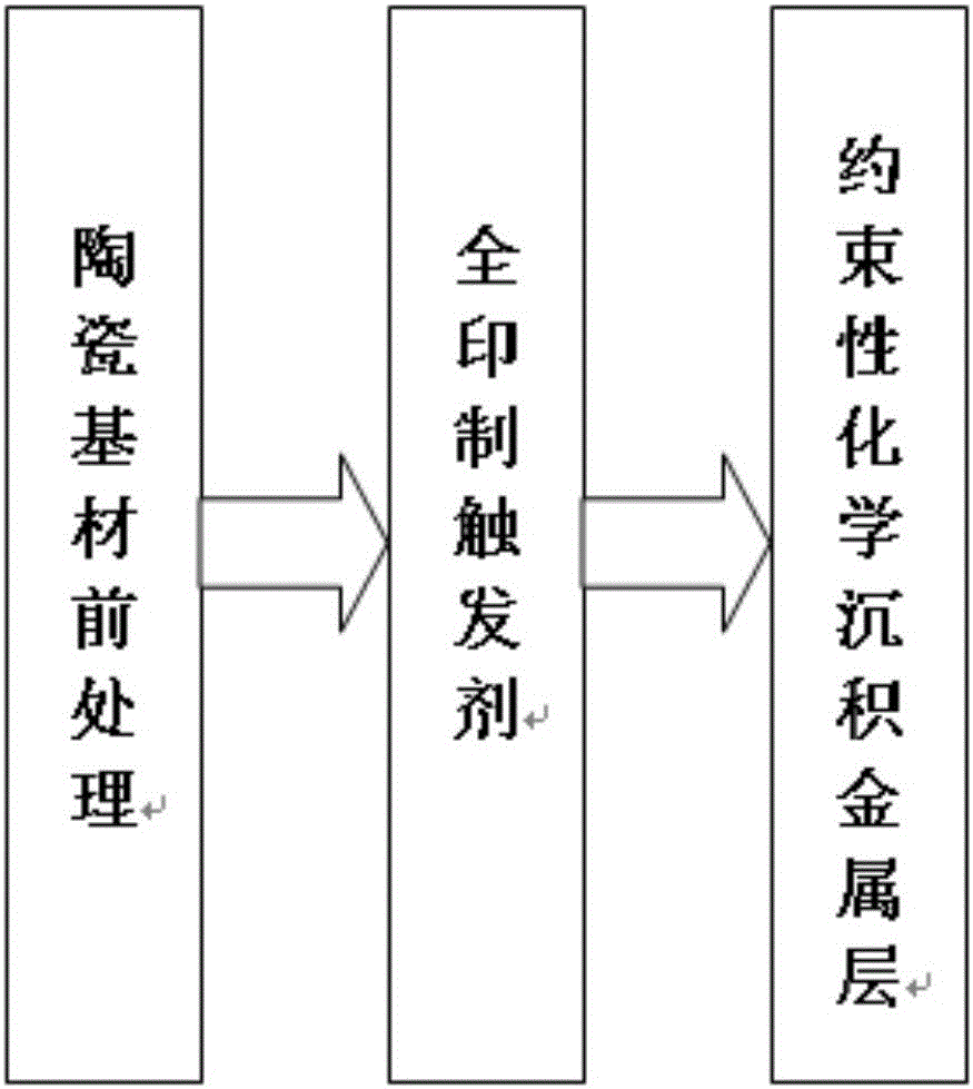
The invention discloses a preparation method of a graphical metal layer on a ceramic surface. The preparation method comprises the following steps: sequentially carrying out pre-cleaning, coarsening, post-cleaning, drying, trigger printing, graphical curing, constrained chemical deposition of a metal layer and the like on the surface of a ceramic substrate; and carrying out constrained chemical deposition of conductive graphics of copper, silver, nickel and alloys thereof on the ceramic surface. The graphical metal layer on the ceramic surface prepared by the preparation method disclosed by the invention is uniform and compact, good in adhesive force and easy to weld, and the electrical properties can satisfy the industrial requirements, and meanwhile, the preparation method disclosed by the invention has the characteristics of simple process, low cost, convenience in industrialized production and the like.

Description

technical field [0001] The invention belongs to the technical field of electronic component manufacturing, and in particular relates to the printing preparation technology of a patterned metal layer on the surface of an electronic ceramic substrate / substrate. The present invention is based on the idea of ​​"additive method", uses the printing method to prepare the required conductive pattern on the surface of the electronic ceramic substrate / substrate, and forms conductive patterns of copper, silver, nickel and their alloys, which can be applied to the metallization of magnetoelectric elements Electrode preparation, LTCC surface and multi-layer wiring, power modules, high-power integrated circuit ceramic substrate wiring, power electronic modules, high thermal conductivity LED ceramic substrate wiring and other fields. Background technique [0002] Components / components based on electronic ceramic substrates / substrates have the characteristics of high hardness, wear resistan...

Claims


Application Information

Patent Timeline
Patent Type & Authority Patents(China)
IPC IPC(8): H05K3/10C04B41/88
Inventor 冯哲圣陈金菊李金彪赵焕芬杨超杨修宇
Owner 遂宁迪印科技有限公司
Learn More